Method for forming a pattern on a substrate and electronic device formed thereby

a technology of electronic devices and substrates, applied in the direction of solid-state devices, semiconductor devices, thermoelectric devices, etc., can solve the problems of incompatibility with continuous in-line manufacturing, high cost of required equipment, and the resolution of the current 20-micrometer-scale device is limited, so as to achieve low cost and low cost

Inactive Publication Date: 2010-06-17
BASF AG
View PDF19 Cites 10 Cited by
  • Summary
  • Abstract
  • Description
  • Claims
  • Application Information

AI Technical Summary

Benefits of technology

[0013]It is an object of the invention to provide a method for forming a pattern on a substrate that overcomes the drawbacks of the known methods discussed above. The method should be suitable for employment in the fields of large-area and / or low-cost electronics. The field of large-area electronics, also macro-electronics, relates to devices with electronic functionality distributed over large areas. A backplane for a large flat panel display, which requires a switching transistor behind each pixel, constitutes a typical example. The field of low-cost electronics relates to application areas and electronic devices for which silicon technology is prohibitive due to cost reasons, an example being an item level RFID (radio-frequency identification) tag that can be used as electronic barcode. Large-area and / or low-cost electronics require large-area compatible and / or low-cost materials such as hydrogenated amorphous silicon or organic semiconductors. Furthermore, methods for forming a pattern on a substrate are required that offer the necessary resolution, registration accuracy, robustness, cost-effectiveness and, in particular, throughput to be viable for large-area and / or low-cost electronic components.

Problems solved by technology

The methods are based on a step-and-repeat process and are thus not compatible with continuous in-line manufacturing.
At the moment, a throughput of 10−3 m2 / s, which corresponds to 50,000 300 millimeter wavers per month, can be achieved with these lithographic methods, the required equipment being rather expensive.
Processes employing these print technologies offer a throughput of several m2 / s but their resolution is currently limited to 20 micrometers or more, which is usually not sufficient for electronic applications.
Solid-state embossing is usually quite time consuming and the employed microcutting tool has to be robust, especially for a large-scale production facility.
Because of the ink flow and the drying step micromoulding is a comparably slow process.
The materials, however, have to withstand high temperatures.

Method used


Image

  • Method for forming a pattern on a substrate and electronic device formed thereby
  • Method for forming a pattern on a substrate and electronic device formed thereby
  • Method for forming a pattern on a substrate and electronic device formed thereby

Examples


Embodiment Construction

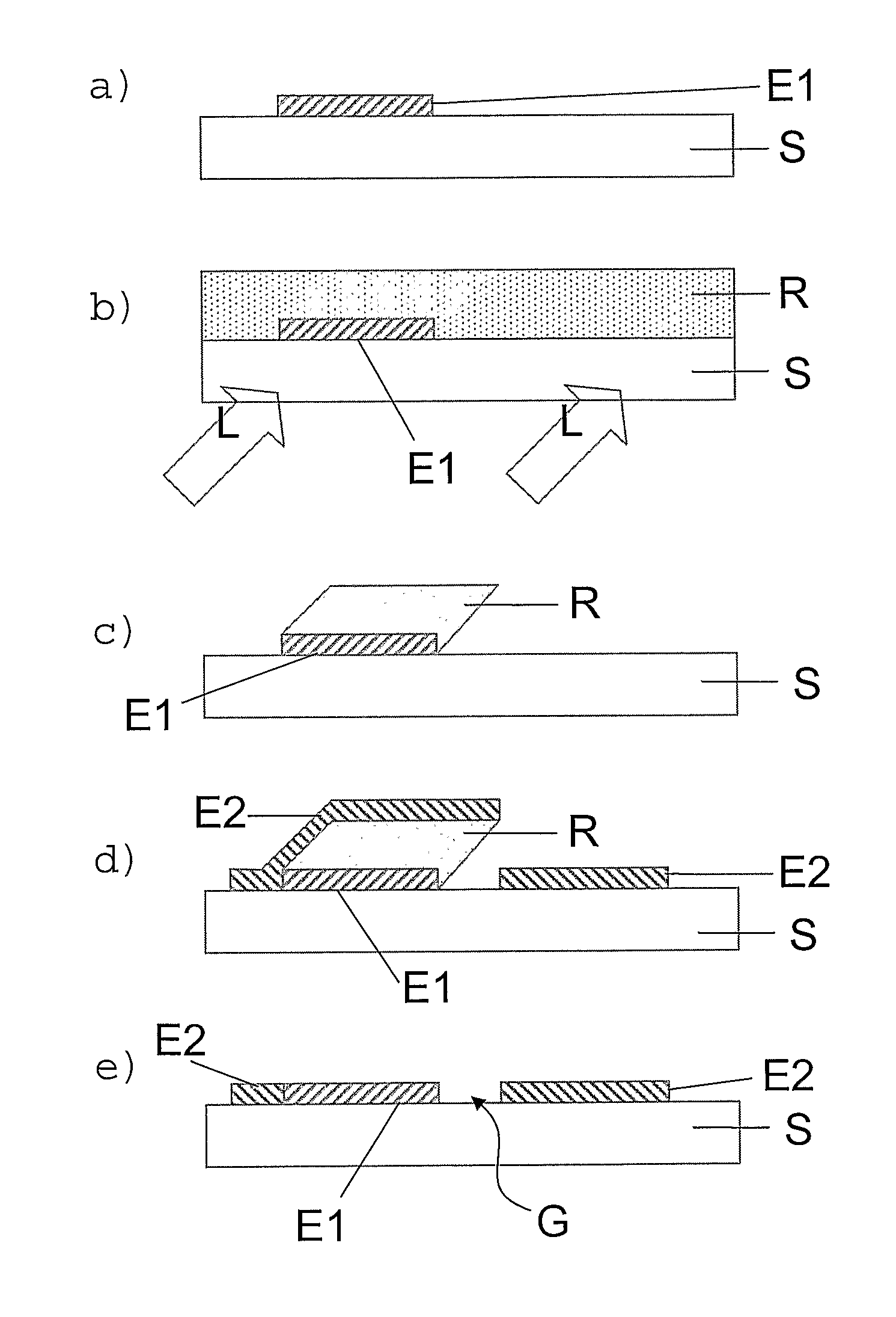
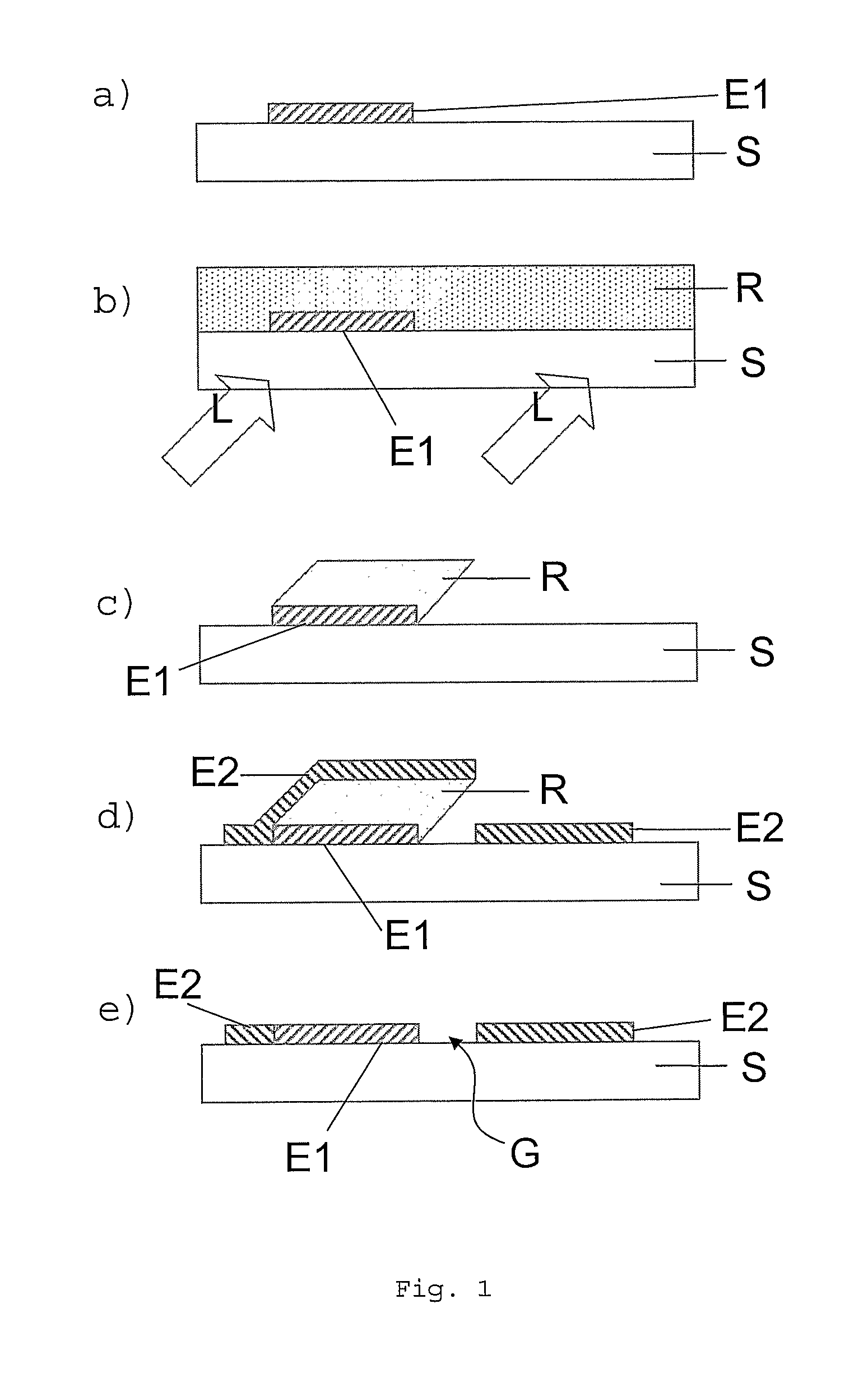
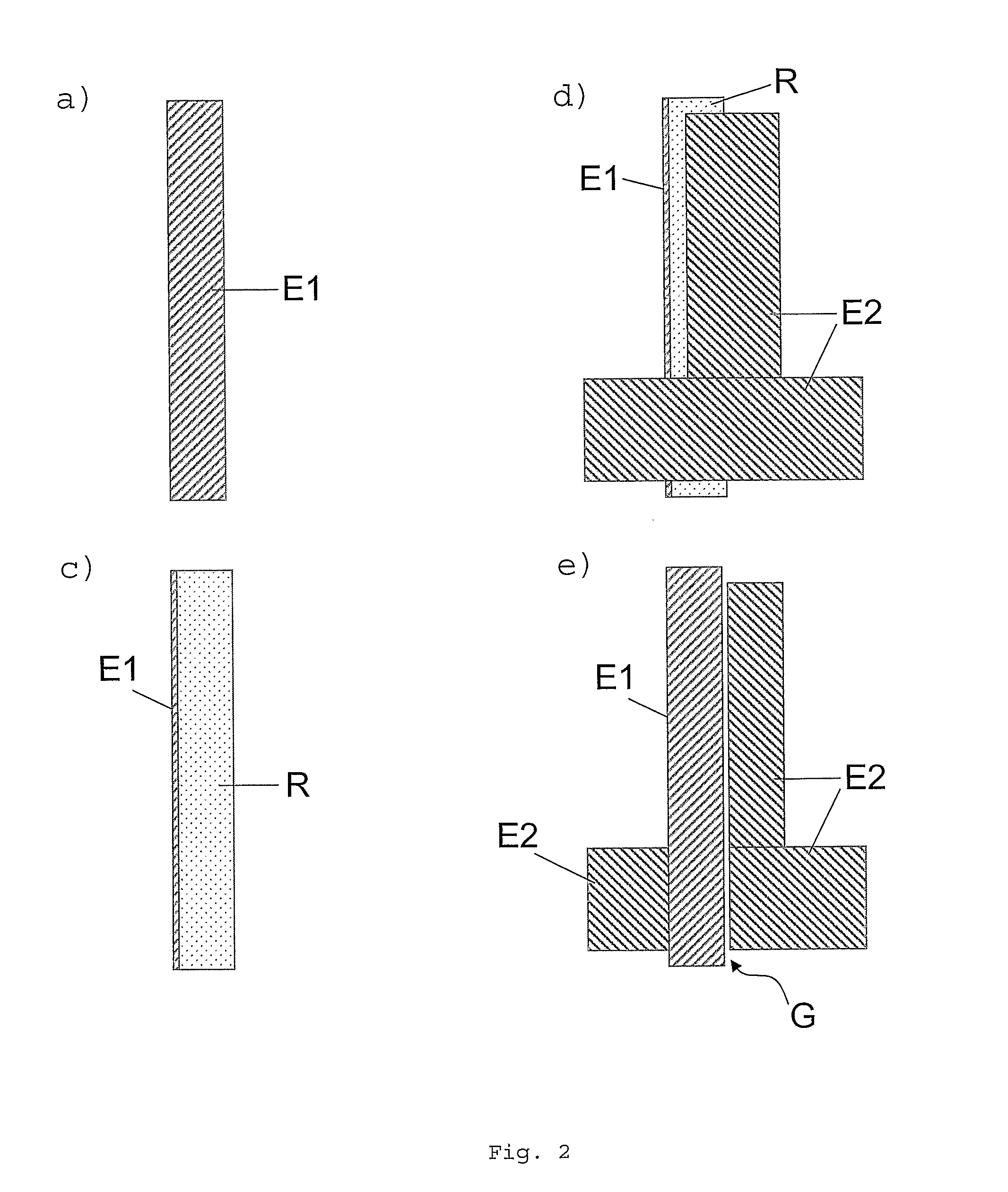
[0037]FIGS. 1 and 2 show schematic representations of the method according to the invention. In a first step (FIGS. 1a and 2a) the first layer E1 of an opaque material is deposited on the upper surface of a substrate S. The substrate S is at least partially transparent, in particular semi-transparent, to a light beam L, the light beam preferably comprising or consisting of UV-radiation which is later on needed to expose a photosensitive layer R. The first layer E1 is non-transparent to the light beam L, in particular to UV-radiation. The material of the first layer E1 can for example be an electrical conductor, the first layer E1 then forming an electrode. Suitable pattering techniques such as, for example, so called shadow mask evaporation can be employed for forming the first layer E1 into its desired shape. Preferably additive pattering techniques, which are compatible with roll-to-roll fabrication such as pattering techniques including gravure and ink-jet printing, are employed ...


PUM

PropertyMeasurementUnit
lengthsaaaaaaaaaa
lengthsaaaaaaaaaa
channel lengthaaaaaaaaaa

Abstract

The invention relates to a method for forming a pattern on a substrate (S) with an upper surface and a lower surface which comprises the steps of depositing a first layer (E1) of an opaque material on the upper surface of the substrate (S), depositing a photosensitive layer (R) such that part of the photosensitive layer (R) covers at least part of the first layer (E1), exposing the photosensitive layer (R) to a light beam (L), the light beam (L) impinging on the lower surface of the substrate (S) under an oblique angle (Φ) of incidence, removing the exposed region of the photosensitive layer (R), depositing a second layer (E2) of an opaque material such that part of the second layer (E2) covers a remaining region of the photosensitive layer (R), and removing at least a part of the remaining region of the photosensitive layer (R). According to another aspect of the method of the invention anisotropic plasma etching is applied from above the upper surface of the substrate (S) after removal of the exposed region of the photosensitive layer (R) and thereafter the second layer (E2) is deposited. The method of the invention can be applied for forming a source electrode and a drain electrode of a thin-film field effect transistor. The invention furthermore relates to an electronic device fabricated by such a method.

Description

CROSS REFERENCES TO RELATED APPLICATIONS[0001]This application claims the priority of European patent application 07 007 990.0, filed on Apr. 19, 2007, the disclosure of which is incorporated herein by reference in its entirety.TECHNICAL FIELD[0002]The invention relates to a method for forming a pattern on a substrate and to an electronic device formed thereby. The electronic device may in particular be an organic electronic device.BACKGROUND ART[0003]For forming patterns in structures in the micrometer and sub-micrometer range for electronic and micro technology applications usually methods relying on electron beam, X-ray, ion beam and optical lithography are employed. With these lithographic methods a resolution of 1 micrometer or better can be achieved. The methods are based on a step-and-repeat process and are thus not compatible with continuous in-line manufacturing. At the moment, a throughput of 10−3 m2 / s, which corresponds to 50,000 300 millimeter wavers per month, can be ac...

Claims


Application Information

Patent Timeline
Patent Type & Authority Applications(United States)
IPC IPC(8): H01L51/05H01L21/336H01L21/027H01L51/42H01L51/50
CPCH01L21/0272H01L21/0274H01L21/0335Y02E10/549H01L51/0037H01L51/0097H01L51/0512H01L51/0018H10K71/233H10K85/1135H10K10/462H10K77/111H10K71/231
Inventor BURGI, LUKASPFEIFFER, RETOWALTER, HARALDVON MUHLENEN, ADRIAN
Owner BASF AG
Why Eureka
Try Eureka