Method for gate leakage reduction and Vt shift control and complementary metal-oxide-semiconductor device

a technology of metal oxides and semiconductors, applied in the field of complementary metal oxidesemiconductor devices, can solve the problems of reducing the vt, nmos or pmos serious shift, and increasing the difference between the equivalent oxide thickness (eot) of the gate dielectric layer of the pmos transistor and the eot of the gate dielectric layer of the nmos transistor, so as to suppress vt shift and effectively reduce the effect of gate leakag

Active Publication Date: 2010-06-17
UNITED MICROELECTRONICS CORP
View PDF27 Cites 26 Cited by
  • Summary
  • Abstract
  • Description
  • Claims
  • Application Information

AI Technical Summary

Benefits of technology

[0008]The main objective of the present invention is to provide a method for gate leakage reduction and Vt shift control, to effectively reduce gate leakage often encountered by a thin gate dielectric layer and to suppress Vt shift often caused by nitridation of gate dielectric layer, and, in the same time, to avoid the problem induced by the difference of the EOT between the PMOS and the NMOS transistors.

Problems solved by technology

However, high nitride dose of SiON gate dielectric will lead the threshold voltage, Vt, of NMOS or PMOS to seriously shift.
Unfortunately, the fluorine implantation after polysilicon gate electrode deposition induces a new problem, that is, the difference between the equivalent oxide thickness (EOT) of the gate dielectric layers of the PMOS transistor and the EOT of the gate dielectric layer of the NMOS transistor will increase with the increase of fluorine implantation after polysilicon gate electrode deposition.

Method used


Image

  • Method for gate leakage reduction and Vt shift control and complementary metal-oxide-semiconductor device
  • Method for gate leakage reduction and Vt shift control and complementary metal-oxide-semiconductor device
  • Method for gate leakage reduction and Vt shift control and complementary metal-oxide-semiconductor device

Examples


example

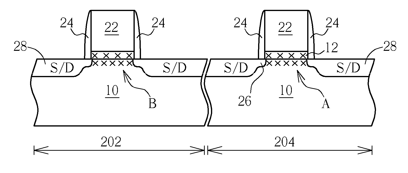
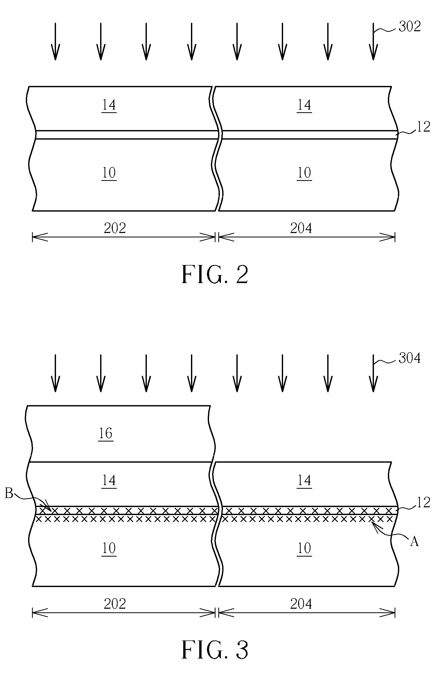
[0039]CMOS devices were made on six wafers numbered as #1 to #6 using the method of the present invention. A gate oxide layer with a thickness of 16 Å was formed on each of the wafers #1 to #5, and a gate oxide layer with a thickness of 15 Å was formed on the wafer #6, followed by a DPN process carried out on the gate oxide layers. For the wafer #6, a pressure of 10 mTorr, a power of 1000 W (effective power 200 W (200 W Eff)), duty cycle (DC): 20%, and a nitrogen dosage of 4.0×10¹⁵ atoms / cm2 were used to carry out the DPN process for 80 seconds. For the wafers #1 to #5, a pressure of 10 mTorr, a power of 2500 W (500 W Eff), DC: 20%, and a nitrogen dosage of 4.5×10¹⁵ atoms / cm2 were used to carry out the DPN process. Thereafter, the six wafers were subjected to a post nitridation annealing (PNA) process at 1100° C., with a flow ratio of nitrogen / oxygen being as 6 / 2.4 L / L, under a pressure of 50 Torr, for 35 seconds. Thereafter, a polysilicon layer with a thickness of 800 Å was formed ...


PUM


Abstract

The present invention relates to a method for gate leakage reduction and Vt shift control, in which a first ion implantation is performed on PMOS region and NMOS region of a substrate to implant fluorine ions, carbon ions, or both in the gate dielectric or the semiconductor substrate, and a second ion implantation is performed only on the NMOS region of the substrate to implant fluorine ions, carbon ions, or both in the gate dielectric or the semiconductor substrate in the NMOS region, with the PMOS region being covered by a mask layer. Thus, the doping concentrations obtained by the PMOS region and the NMOS region are different to compensate the side effect caused by the different equivalent oxide thickness and to avoid the Vt shift.

Description

BACKGROUND OF THE INVENTION [0001]1. Field of the Invention[0002]The present invention relates to a technology concerning complementary metal-oxide-semiconductor (CMOS) devices, and particularly to a method for gate leakage reduction and Vt shift control for a CMOS device and a CMOS device made by such method.[0003]2. Description of the Prior Art[0004]Along with MOS device miniaturization, gate dielectric has been scaled aggressively, but gate leakage will be increased while gate dielectric thickness is thinning down. Nitride dose of SiON gate dielectric is increased through a decoupled-plasma nitridation (DPN) treatment to meet the demand of thin gate dielectric with low gate leakage. In other words, the DPN process is used to improve robustness of ultra thin gate dielectrics and to efficiently reduce the gate leakage, as well as to offer a better barrier to boron. However, high nitride dose of SiON gate dielectric will lead the threshold voltage, Vt, of NMOS or PMOS to seriously s...

Claims


Application Information

Patent Timeline
Patent Type & Authority Applications(United States)
IPC IPC(8): H01L27/092H01L21/426
CPCH01L21/823857H01L21/823807
Inventor LIN, CHIEN-LIANGWANG, YU-RENKAO, WU-CHUNLI, YING-HSUANYEN, YING-WEICHAN, SHU-YEN
Owner UNITED MICROELECTRONICS CORP
Why Eureka
Try Eureka