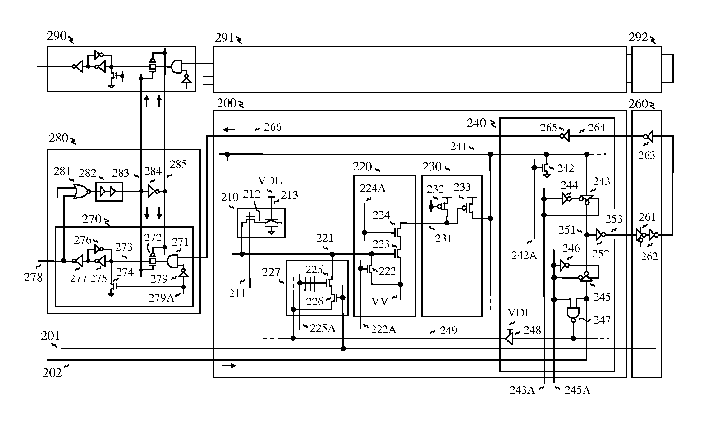
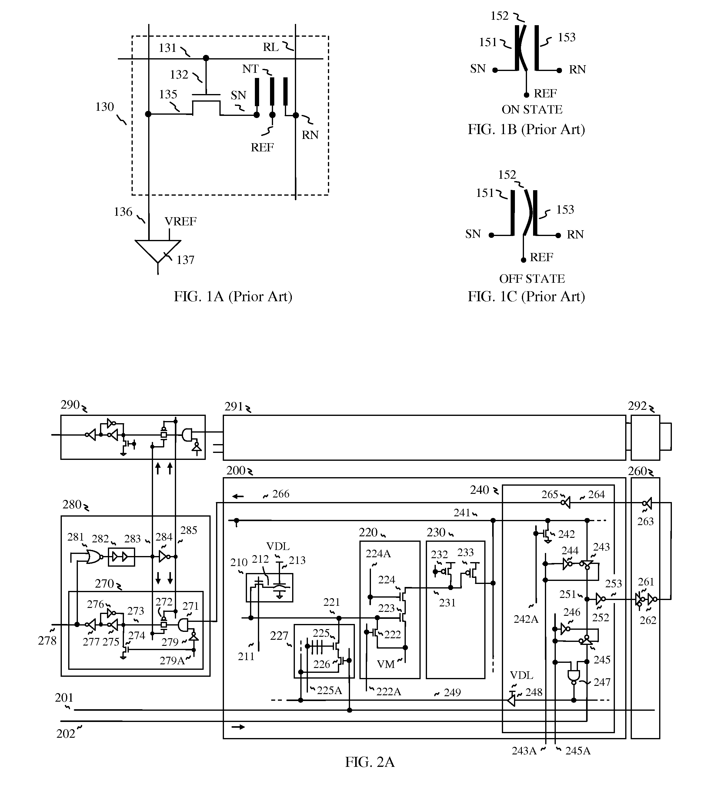
[0009]For realizing high speed carbon nanotube memory, local bit line is multi-divided into short line for reducing
parasitic capacitance, which realizes fast read / write operation with
fast charging / discharging time. And, a small local sense amp is realized for reading a data in a memory
cell through lightly loaded local bit line, such that the local sense amp is composed of a local write circuit, a local pre
amplifier and a local main amplifier, where a source line of the local pre amplifier is connected to a middle
voltage VM as a reference
voltage for detecting whether the local bit line is higher than that of the VM voltage which is also forced to the local bit line as a pre-
charge voltage. In doing so, no
waiting time is required for enabling the local pre amplifier after a word line is turned on, because the local pre amplifier discharges a local pre-amp node when reading data “1”, otherwise the local pre amplifier does not
discharge the local pre-amp node, when reading data “0”. And a global sense amp is connected to the local sense amp through a read global bit line for reading an output of the local sense amp.
[0011]And, configuring memory is more flexible, such that multiple memory macros can be easily configured with small segmented
memory array and multi-stage sense amps, instead of big
macro with the conventional sense amps. And number of sense amps can be determined by the target speed. For example, high speed application needs more segmented array with more sense amps, while
high density application needs more memory cells with reduced number of sense amps, thus
cell efficiency is increased.
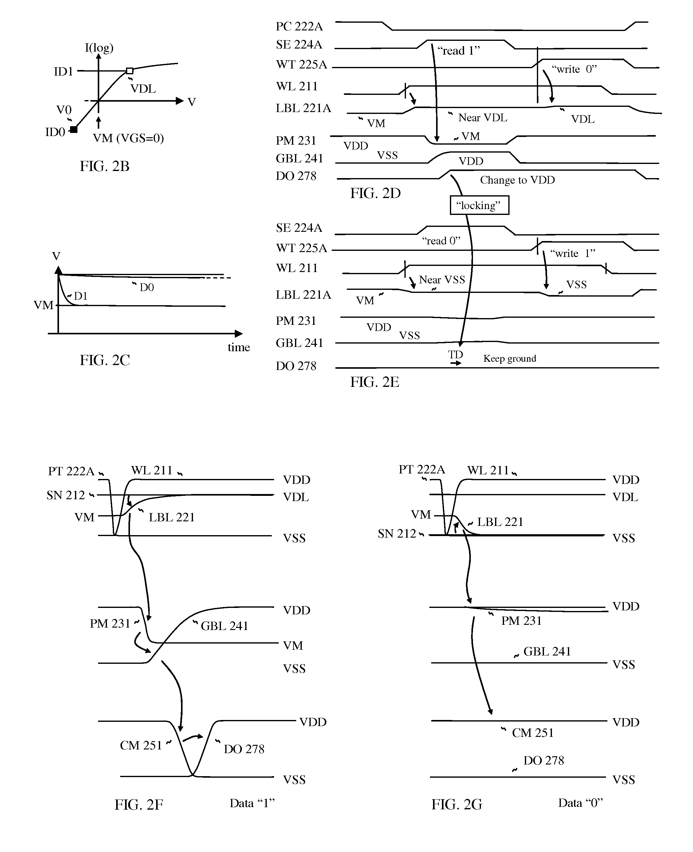
[0014]More specifically, a reference
signal is generated by one of fast changing data with high
gain from reference cells, which
signal serves as a reference
signal to generate a locking signal for the output latch circuit in order to reject latching another data which is slowly changed with
low gain, such that
high voltage data is arrived first while
low voltage data is arrived later, or
low voltage data is arrived first while
high voltage data is arrived later depending on configuration. The time-domain sensing scheme effectively differentiates high voltage data and low voltage data with time
delay control, while the conventional sensing scheme is current-domain or voltage-domain sensing scheme with a heavy bit
line pair. There are many advantages to realize the time-domain sensing scheme, so that the sensing time is easily controlled by a tunable
delay circuit, which compensates cell-to-cell variation and
wafer-to-
wafer variation, such that there is a need for adding a
delay time before locking the output latch circuit with a statistical data for all the memory cells, such as mean time between fast data and slow data. Thereby the tunable delay circuit generates a delay for optimum range of locking time. And the read output from the memory cell is transferred to the output latch circuit through a returning read path, thus the
access time is equal regardless of the location of the selected memory cell, which is advantageous to transfer the read output to the external pad at a time.
[0015]And, the current flow of the pass
transistor of the memory cell can be reduced because the pass transistor only drives a lightly loaded local bit line, which means that the pass transistor can be miniaturized further. Moreover, the present invention realizes multi-stacked memory
cell structure including
thin film transistor because the memory cell only drives lightly loaded bit line even though thin film polysilicon transistor can flow lower current, for example, around 10 times lower. Thereby, bit line loading is reduced around 10 times lower for compensating the low current drivability of the pass transistor. There are almost no limits to stack multiple memory cells as long as the flatness is enough to accumulate the memory cell.
[0017]And the fabrication method is compatible with the conventional
CMOS process for forming the memory cell. In addition, field-effect aligning process is realized for aligning the carbon nanotubes on
exact location of the memory cell, when forming the memory cell. And, the memory cell can be formed from thin film polysilicon layer alternatively, because the lightly loaded bit line can be quickly discharged by the memory cell even though the thin film pass transistor can flow relatively low current. In doing so, multi-stacked memory is realized with
thin film transistor, which can increase the density within the conventional
CMOS process with additional process steps, because the conventional
CMOS process is almost reaching to a scaling limit for fabricating transistors on a surface of a
wafer. And, a body-tied TFT (
Thin Film Transistor) transistor can be alternatively used as the
thin film transistor for alleviating
self heating problem of short channel TFT. In doing so, multi-stacked memory is realized with short channel TFT transistor.

