Surface plasmon-enhanced photovoltaic device

a surface plasmon and photovoltaic technology, applied in the direction of semiconductor devices, electrical equipment, nanotechnology, etc., can solve the problems of preventing large-scale commercialization of these devices, the cost of pv has come down by several orders of magnitude, and the cost of pv remains in the pv module itself, so as to achieve the effect of convenient processing, low cost and advantageous opto-electronic properties

Active Publication Date: 2010-07-15
RGT UNIV OF CALIFORNIA
View PDF2 Cites 26 Cited by
  • Summary
  • Abstract
  • Description
  • Claims
  • Application Information

AI Technical Summary

Benefits of technology

[0006]The present invention provides innovative photovoltaic devices driven by intense photoemission of “hot” electrons from a suitable nanostructured metal. The metal should be an electron source with surface plasmon resonance within the visible and near-visible spectrum range (near IR to near ...

Problems solved by technology

However, the high cost of these devices prevented large-scale commercialization for many years.
In the last twenty-five years, the c...

Method used


Image

  • Surface plasmon-enhanced photovoltaic device
  • Surface plasmon-enhanced photovoltaic device
  • Surface plasmon-enhanced photovoltaic device

Examples


Embodiment Construction

[0016]Reference will now be made in detail to specific embodiments of the invention. Examples of the specific embodiments are illustrated in the accompanying drawings. While the invention will be described in conjunction with these specific embodiments, it will be understood that it is not intended to limit the invention to such specific embodiments. On the contrary, it is intended to cover alternatives, modifications, and equivalents as may be included within the spirit and scope of the invention as defined by the appended claims. In the following description, numerous specific details are set forth in order to provide a thorough understanding of the present invention. The present invention may be practiced without some or all of these specific details. In other instances, well known process operations have not been described in detail so as to not unnecessarily obscure the present invention.

[0017]Introduction

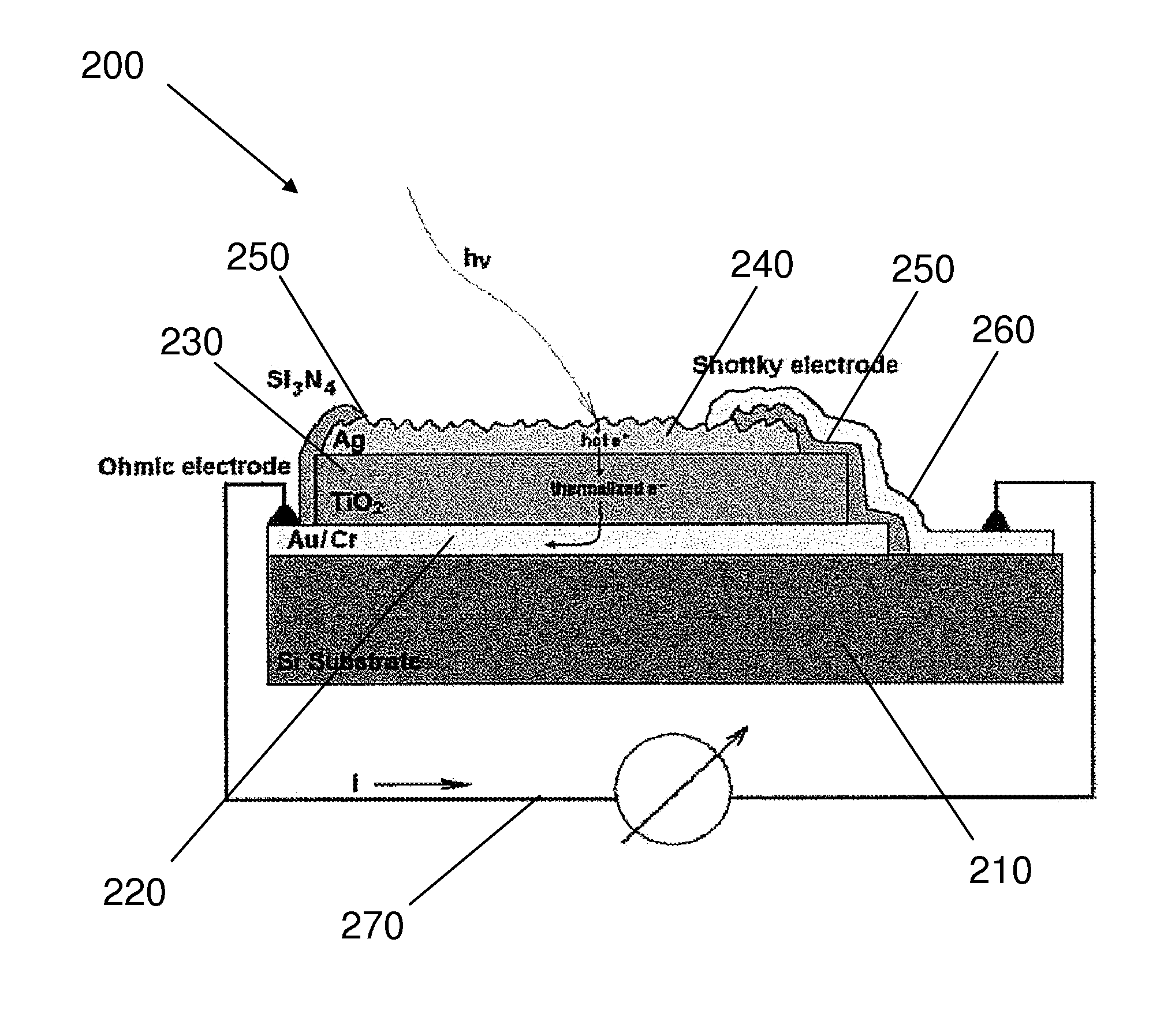
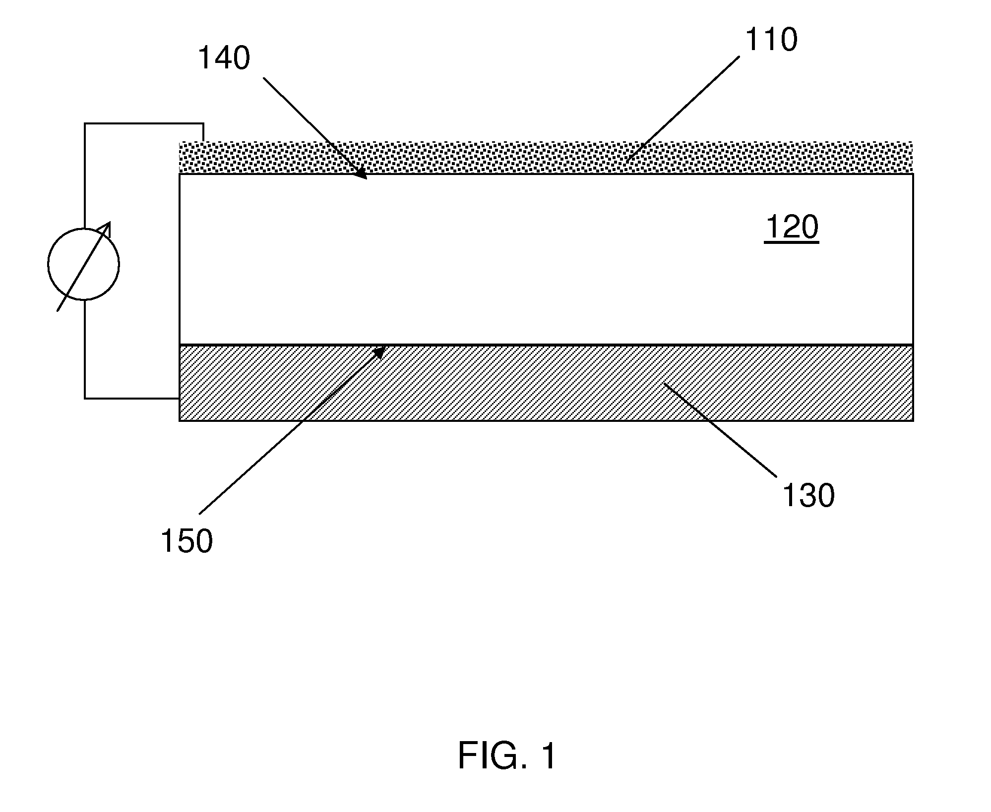
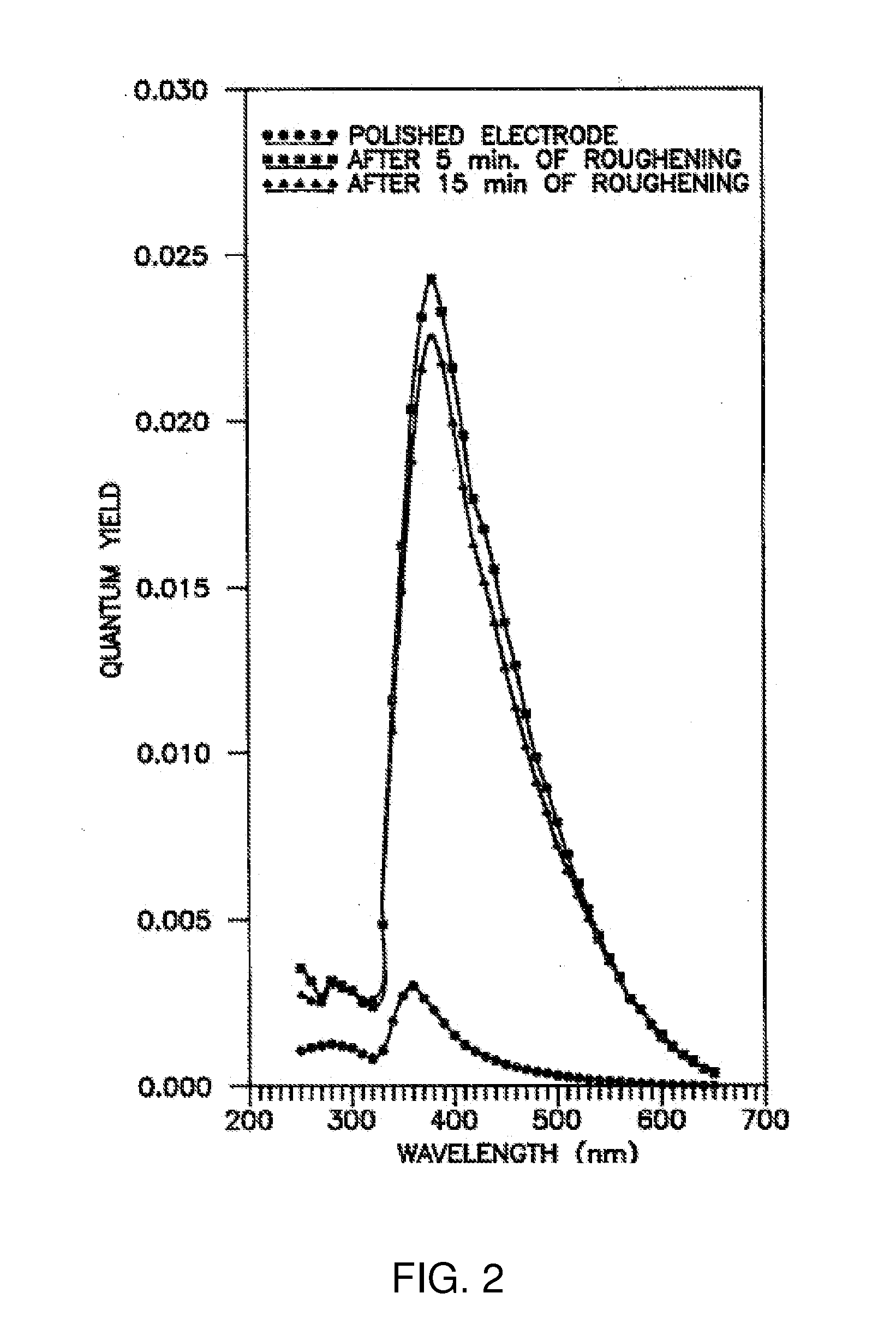
[0018]The present invention provides innovative photovoltaic devices driv...


PUM


Abstract

Photovoltaic devices are driven by intense photoemission of “hot” electrons from a suitable nanostructured metal. The metal should be an electron source with surface plasmon resonance within the visible and near-visible spectrum range (near IR to near UV (about 300 to 1000 nm)). Suitable metals include silver, gold, copper and alloys of silver, gold and copper with each other. Silver is particularly preferred for its advantageous opto-electronic properties in the near UV and visible spectrum range, relatively low cost, and simplicity of processing.

Description

CROSS-REFERENCE TO RELATED APPLICATIONS[0001]This application claims priority to U.S. Provisional Patent Application No. 60 / 950,557, titled SURFACE PLASMON-ENHANCED PHOTOVOLTAIC DEVICE, filed Jul. 18, 2007, the disclosure of which is incorporated herein by reference in its entirety and for all purposes.STATEMENT OF GOVERNMENTAL SUPPORT[0002]The invention described and claimed herein was made at least in part utilizing funds supplied by the U.S. Department of Energy under Contract No. DE-AC02-05CH11231. The Government has certain rights in this invention.BACKGROUND OF THE INVENTION[0003]Solar energy is clean, abundant, widespread and renewable. Various technologies exist for capturing solar energy, concentrating it, storing it, and converting it into other useful forms of energy. Solar energy technologies have great potential benefit in that they can diversify energy supply, reduce dependence on fossil fuels, offset greenhouse gas emissions and improve air quality.[0004]Edmond Becque...

Claims


Application Information

Patent Timeline
IPC IPC(8): H01L31/108H01L31/0352H01L31/18
CPCB82Y10/00H01L31/035281Y02E10/50H01L31/07H01L31/1085H01L31/03529
Inventor KOSTECKI, ROBERTMAO, SAMUEL S.
Owner RGT UNIV OF CALIFORNIA
Why Eureka
Try Eureka