Near-infrared imaging sensor

a sensor and near-infrared technology, applied in the field of near-infrared imaging sensors, can solve the problems of low yield, difficult stable manufacture, complicated image pickup system, etc., and achieve the effects of high yield, high reproducibility, and simple structur

Active Publication Date: 2010-07-22
SUMITOMO ELECTRIC IND LTD
View PDF6 Cites 23 Cited by
  • Summary
  • Abstract
  • Description
  • Claims
  • Application Information

AI Technical Summary

Benefits of technology

[0008]It is an object of the present invention to provide a near-infrared imaging sensor which is simple in structure, which can uniformly transmit near-infrared light without depending on the wavelength, and which can be manufactured at high yield with high reproducibility. It is another object of the present invention to provide a method for manufacturing such a near-infrared imaging sensor.

Problems solved by technology

(1) and (2): (i) Since an image sensor used requires an optical lens, a filter, and the like, an image pickup system is complicated and has a large size.
(ii) Since an increased number of components are necessary and high alignment accuracy is required to assemble a complicated structure, stable manufacture is difficult and yield is low.
It is difficult to use glass to fabricate a micro-structure with high precision.

Method used


Image

  • Near-infrared imaging sensor
  • Near-infrared imaging sensor
  • Near-infrared imaging sensor

Examples


Embodiment Construction

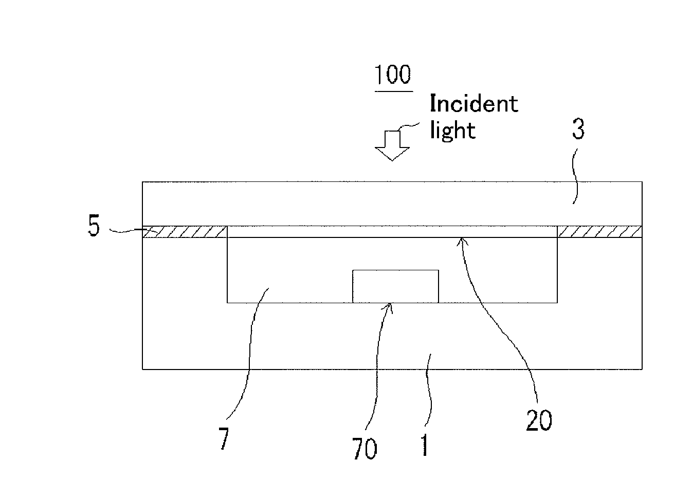
[0036]FIG. 1 is a sectional view of a near-infrared imaging sensor 100 according to an embodiment of the present invention. A sensor chip-mounted body 70 includes a photodiode array 50 and a multiplexer 71 which is a signal readout circuit (ROIC) and is fixed on the bottom of a housing main body section 1. The housing main body section 1 is, for example, a blind cylinder such as a blind circular cylinder or angular tube. The housing main body section 1 has an opening located on the light-incident side and the opening is covered with a lid 3. The lid 3 is fixed to the housing main body section 1 with a fixing member 5 made of a solder such as a tin (Sn) eutectic alloy. An inner space 7 is vacuum-sealed; hence, the fixing member 5 needs to have sufficient strength and durability. The lid 3 is made of silicon (Si) and has an optical component 20 disposed on an inner surface thereof.

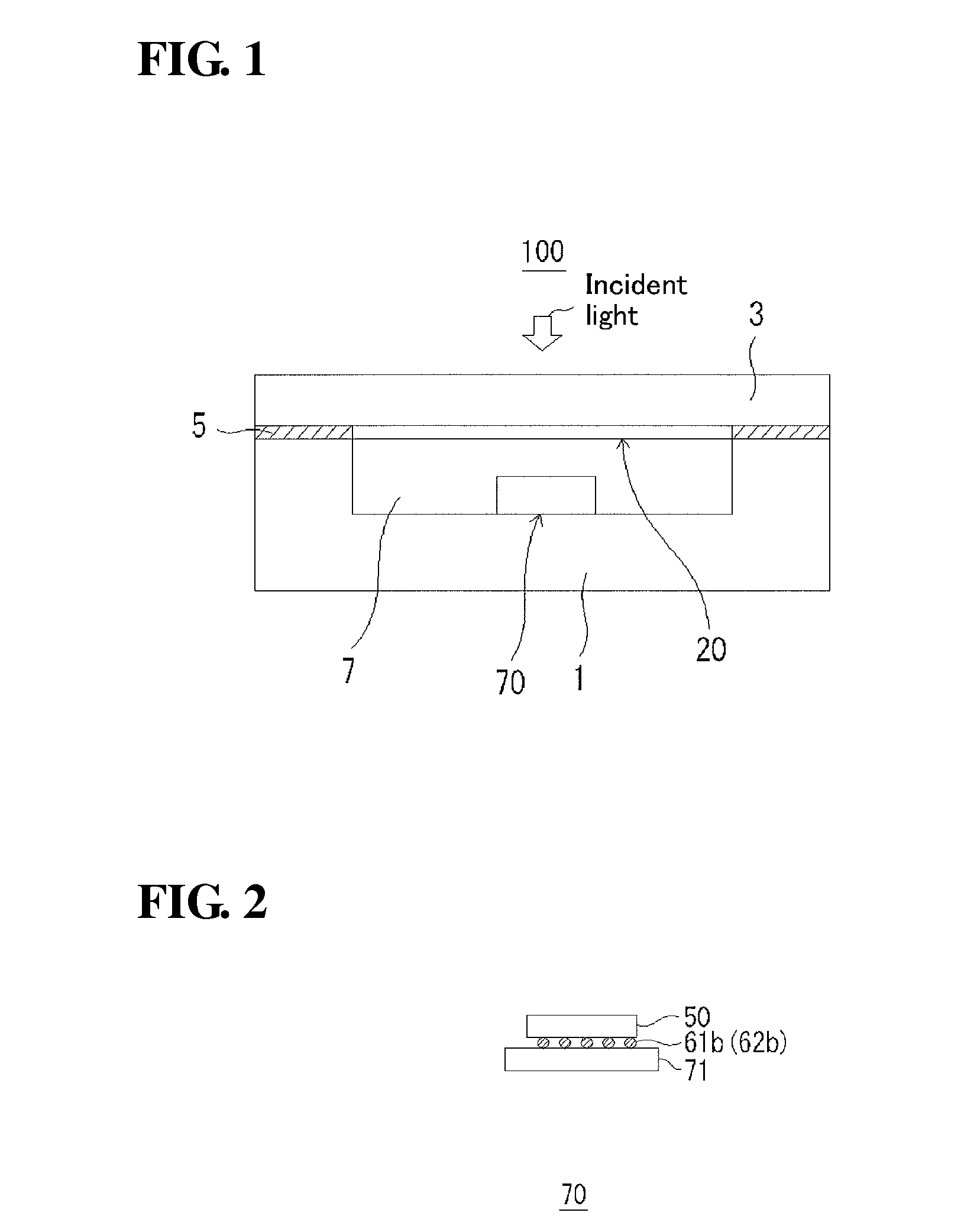
[0037]FIG. 2 is a schematic view of the sensor chip-mounted body 70. In the sensor chip-mounted body 70, ...


PUM


Abstract

A near-infrared imaging sensor according to the present invention includes a photodiode array sensitive to light with a wavelength of 1.2 to 3 μm and a multiplexer including a signal readout circuit. The near-infrared imaging sensor is contained in a housing and is vacuum-sealed. The housing includes a main body section and a lid covering the main body section. The lid is made of a material transparent to light with a wavelength of 1.2 to 3 μm.

Description

BACKGROUND OF THE INVENTION[0001]1. Field of the Invention[0002]The present invention relates to a near-infrared imaging sensor sensitive to near-infrared light.[0003]2. Description of the Related Art[0004]Infrared absorption bands of living organisms, foods, and the like are in the near-infrared range and therefore near-infrared imaging sensors are expected to be used for various applications in many surrounding fields. A known compound semiconductor which is sensitive to near-infrared light and which operates at room temperature is Indium gallium arsenide (InGaAs), which can detect light with a wavelength of up to 1.7 μm and is insensitive to light with a wavelength of more than 1.7 μm. Light with a wavelength of more than 1.7 μm can be detected with lead sulfide (PbS) and mercury cadmium telluride (HgCdTe, or MCT), which have low sensitivity and need to be cooled as disclosed in a non-patent document such as Masao Nakayama, “Sekigaisen Kenshutsusoshi no Gijutsu DoKo”, Sensor Tech...

Claims


Application Information

Patent Timeline
Patent Type & Authority Applications(United States)
IPC IPC(8): H01L27/146
CPCG02B5/1876H01L27/14618H01L27/14694H01L27/14649H01L27/14625H01L2924/0002H01L2924/00
Inventor INADA, HIROSHINAGAI, YOUICHI
Owner SUMITOMO ELECTRIC IND LTD
Why Eureka
Try Eureka