Semiconductor storage device

a technology of semiconductor devices and storage devices, applied in semiconductor devices, digital storage, instruments, etc., can solve problems such as increasing the area of cells, and achieve the effects of increasing storage capacity, high reliability, and reducing the size of memory cells

Active Publication Date: 2010-07-22
HITACHI LTD
View PDF9 Cites 54 Cited by
  • Summary
  • Abstract
  • Description
  • Claims
  • Application Information

AI Technical Summary

Benefits of technology

[0015]When the transistor in the nonselective memory is turned on as with the read operation, a write or erase voltage to be applied between both ends of the variable resistive device is not applied by the transistor of the on-state. As a result, storage (write and erase) of data can be selectively inhibited. That is, the amplitude and pulse width of a voltage pulse applied between both ends of the memory cell as the variable resistive device are appropriately adjusted, and a high-speed writable and erasable material is selected, thereby enabling the high-speed write and erase to be realized. In addition, there can be provided the nonvolatile semiconductor storage device with high reliability without need for allowing a large current to flow during write / erase operation. FIGS. 4 and 5 are circuit diagrams showing the configuration of a nonvolatile semiconductor storage device according to an embodiment of the present invention. FIGS. 4 and 5 are circuit diagrams showing a case in which plural memory cell arrays is arranged three-dimensionally vertically and in an array, respectively.
[0016]According to an aspect of the present invention, there can be provided the semiconductor storage device that is capable of further reducing the size of the memory cells, and increasing the storage capacity.

Problems solved by technology

However, because one switching transistor exists in each cell, there arises such a problem that the cell area increases.

Method used


Image

  • Semiconductor storage device
  • Semiconductor storage device
  • Semiconductor storage device

Examples


embodiment

[0048]A method of manufacturing a phase change memory according to an embodiment will be described with reference to the accompanying drawings.

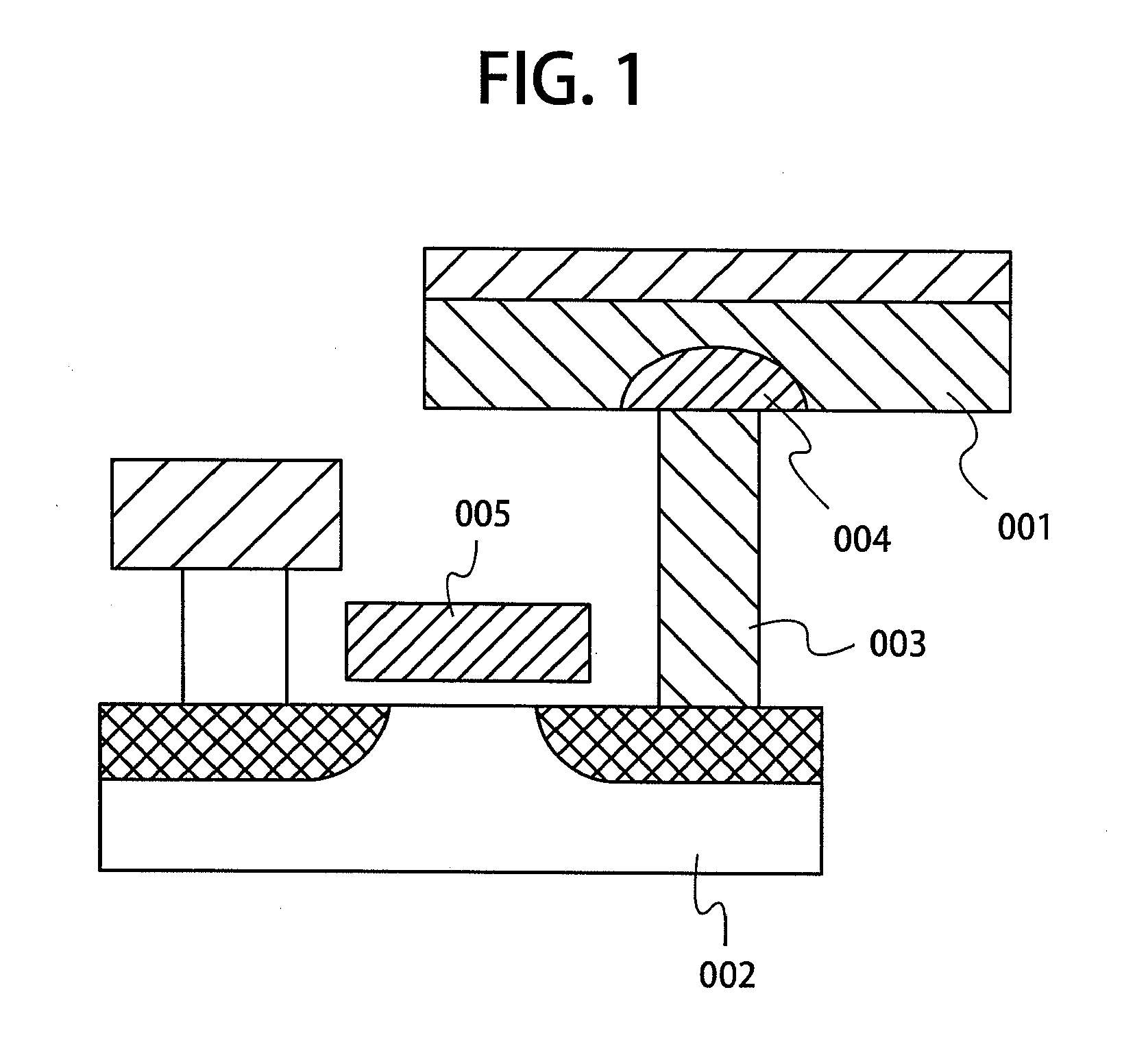
[0049]FIG. 6 shows a cross-sectional view of a memory matrix in which a dopant diffusion layer 101 functioning as a contact layer on a substrate side of a memory cell is formed on a semiconductor substrate 100 including a peripheral circuit, and a first interlayer film 102 and a first polysilicon layer 103 are deposited on the dopant diffusion layer 101 in the stated order. FIG. 7 shows a top view of the memory matrix.

[0050]FIG. 6 is the cross-sectional view taken along a line B-B′ in FIG. 7. The diffusion layer 101 is formed through a known technique such as ion implantation with phosphorus or arsenic as dopant. The diffusion layer 101 may be patterned as a bit line pattern which will be described later, to conduct the operation of selecting a memory cell block. The first interlayer film 102 is made of, for example, oxide film SiO2, and form...


PUM


Abstract

There is provided a semiconductor storage device which is capable of further reducing a size of a memory cell, and increasing a storage capacity. Plural memory cells each including a transistor formed on a semiconductor substrate, and a variable resistive device having a resistance value changed by voltage supply and connected between source and drain terminals of the transistor are arranged longitudinally and in an array to configure a three-dimensional memory cell array. A memory cell structure has a double channel structure in which an inside of a switching transistor is filled with a variable resistance element, particularly, a phase change material. The switching transistor is turned off by application of a voltage to increase a channel resistance so that a current flows in the internal phase change material to operate the memory.

Description

CLAIM OF PRIORITY[0001]The present application claims priority from Japanese patent application JP 2009-008861 filed on Jan. 19, 2009, the content of which is hereby incorporated by reference into this application.BACKGROUND OF THE INVENTION[0002]1. Field of the Invention[0003]The present invention relates to a semiconductor storage device, and more particularly to an electrically rewritable phase-change large capacity memory device that nonvolatilely stores a resistance value determined according to a phase change between a crystal state and an amorphous state of a metal compound.[0004]2. Description of the Related Art[0005]One type of nonvolatile storage devices uses the crystal state and the amorphous state of the metal compound as storage information. The storage material as generally used is tellurium compound. A principle in which information is stored by a difference in reflectivity between those states has been widely used in an optical information storage medium such as a D...

Claims


Application Information

Patent Timeline
Patent Type & Authority Applications(United States)
IPC IPC(8): G11C11/00H01L47/00G11C8/00
CPCG11C13/0004G11C13/003G11C2213/71G11C2213/75G11C2213/79H01L27/2454H01L27/2481H01L45/06H01L45/1233H01L45/144H01L45/1625H01L45/1683H10B63/34H10B63/84H10N70/231H10N70/026H10N70/066H10N70/8828H10N70/826
Inventor SHIMA, AKIOSASAGO, YOSHITAKAKINOSHITA, MASAHARUMINE, TOSHIYUKITAKAURA, NORIKATSUMORIKAWA, TAKAHIROKUROTSUCHI, KENZOHANZAWA, SATORU
Owner HITACHI LTD
Why Eureka
Try Eureka