Apparatus, method for depositing thin film on wafer and method for gap-filling trench using the same

a thin film and trench technology, applied in the direction of coatings, chemical vapor deposition coatings, electric discharge tubes, etc., can solve the problems of low deposition rate and high etching rate, inability to achieve good gap-filling capability, and waste of source gas. , to achieve the effect of improving productivity, good gap-filling capability, and reducing the waste of source gas

Inactive Publication Date: 2010-07-29
WONIK IPS CO LTD
View PDF8 Cites 81 Cited by
  • Summary
  • Abstract
  • Description
  • Claims
  • Application Information

AI Technical Summary

Benefits of technology

[0021]According to exemplary embodiments, it is possible to concurrently or alternatively perform deposition and etching of a thin film, so that a thin film with good gap-fill capability can be deposited. Also, the apparatus

Problems solved by technology

However, in a narrow pattern with a large aspect ratio, gap-filling using such an oxide formed with CVD has limitations.
To obtain high gap-fill capability, HDP-CVD requires a low deposition rate and a high etching rate, which causes the problem of a lower layer being undesirably etched also.
However, this method may also cause etching of a lower layer due to non-uniformity of mass-produced reactors.
However, SA-CVD is problematic in that it has a low deposition rate.
However, when the number of source gas types in the ALD method increases, a complicated gas supply line and a plurality of valves for controlling the gas supply line must be established in order to supply the source gases into a reactor.
Accordingly, problems of increased cost for establishing the gas supply line and the valves and having to

Method used


Image

  • Apparatus, method for depositing thin film on wafer and method for gap-filling trench using the same
  • Apparatus, method for depositing thin film on wafer and method for gap-filling trench using the same
  • Apparatus, method for depositing thin film on wafer and method for gap-filling trench using the same

Examples


Embodiment Construction

[0039]The present invention will now be described more fully with reference to the accompanying drawings, in which exemplary embodiments of the invention are shown. The invention may, however, be embodied in many different forms and should not be construed as being limited to the embodiments set forth herein; rather, these embodiments are provided so that this disclosure will be thorough and complete, and will fully convey the concept of the invention to those skilled in the art.

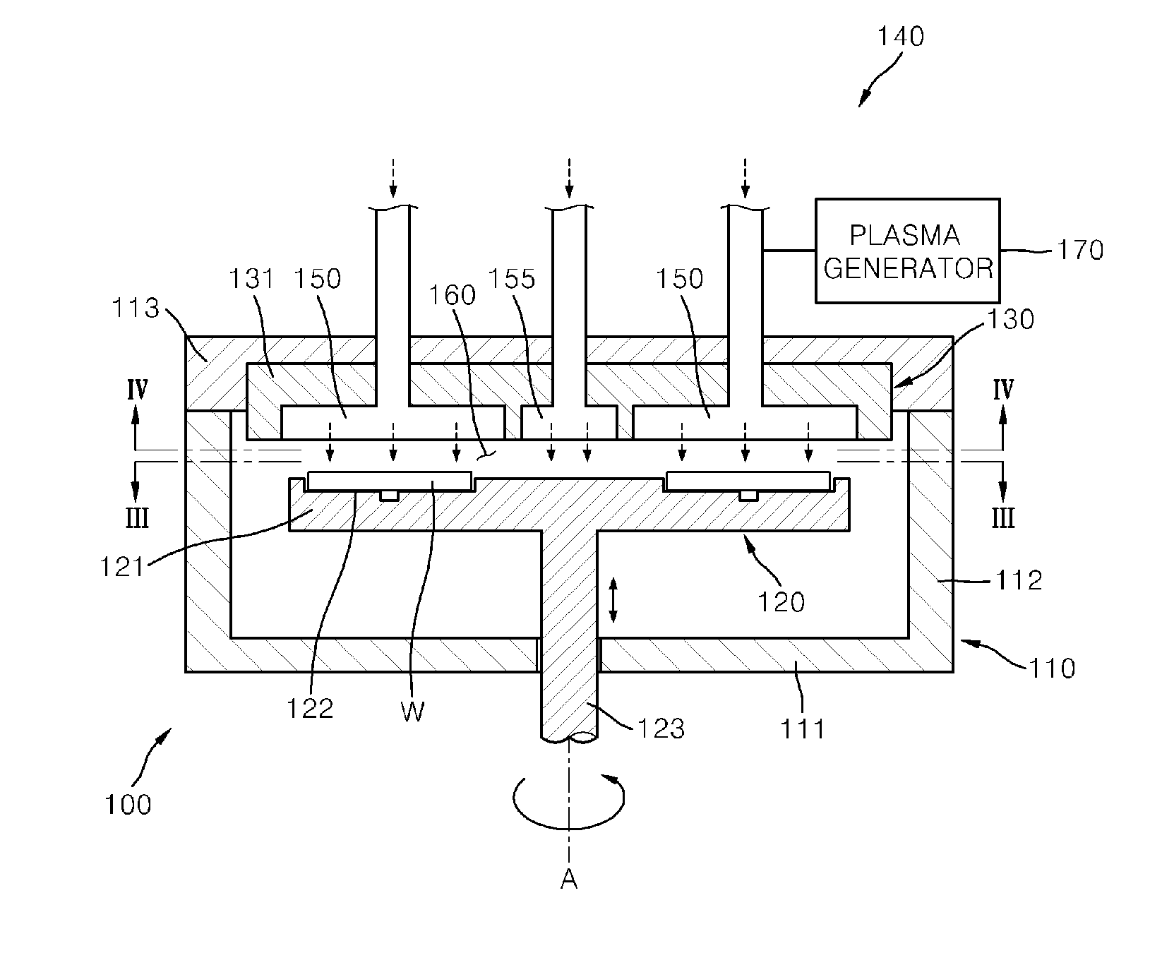
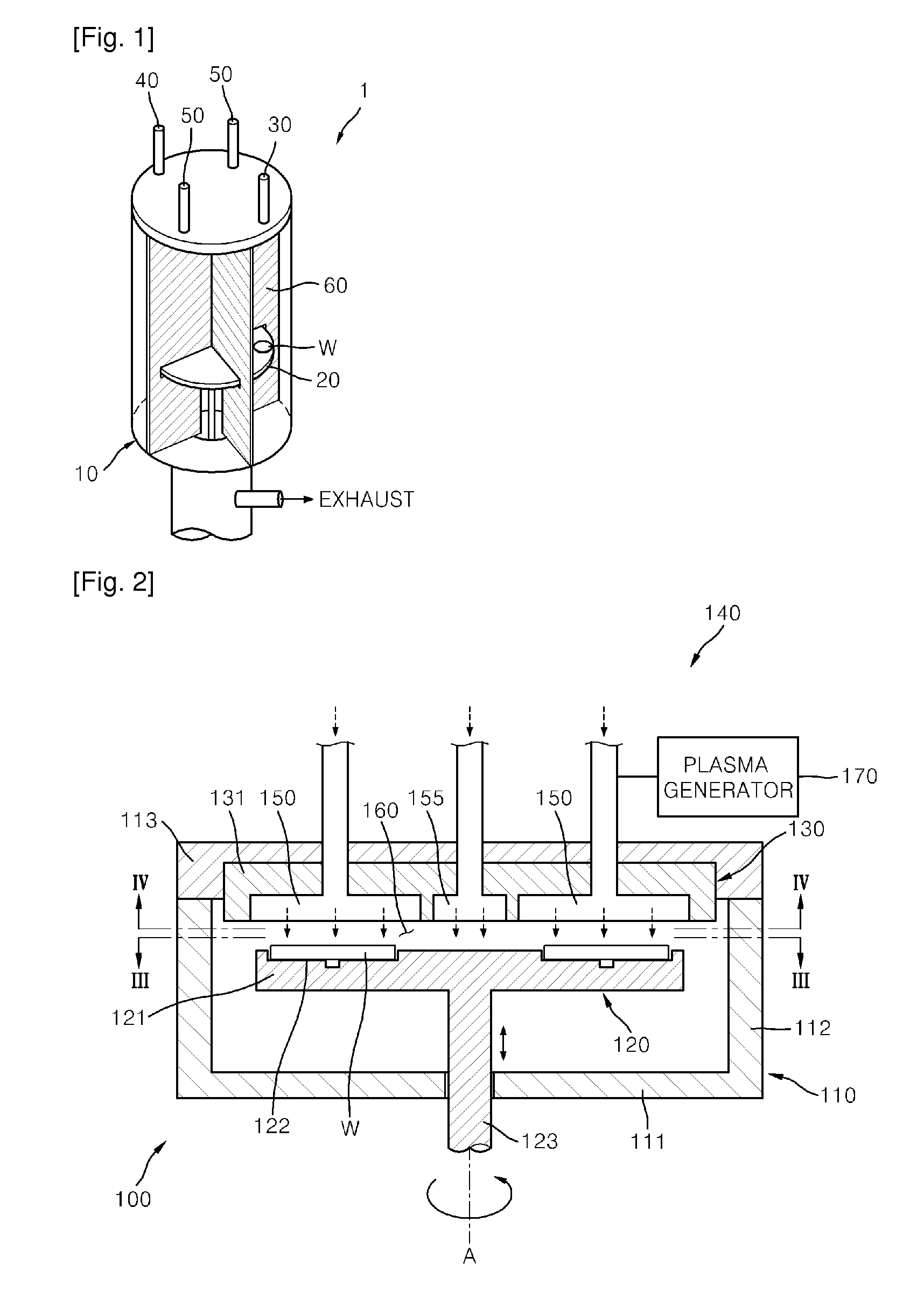
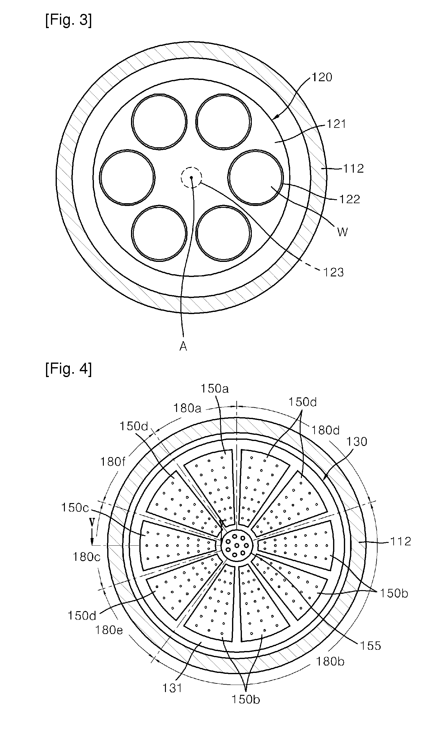
[0040]FIG. 2 is a schematic view of an apparatus for depositing a thin film according to an embodiment of the present invention, FIG. 3 is a sectional view taken along line III-III of FIG. 2, FIGS. 4 and 5 are sectional views taken along line IV-IV of FIG. 2, and FIG. 6 is a sectional view taken along line V-V of FIG. 4.

[0041]Referring to FIGS. 2 to 6, the apparatus for depositing a thin film according to an embodiment of the present invention includes a reactor 110, a substrate supporting plate 120, a gas i...


PUM

PropertyMeasurementUnit
Timeaaaaaaaaaa
Timeaaaaaaaaaa
Flow rateaaaaaaaaaa

Abstract

Provided are an apparatus and method for depositing a thin film, and a method for gap-filling a trench in a semiconductor device. The thin film depositing apparatus includes a plurality of substrates provided on the same space inside a reactor, wherein deposition of the thin film and partial etching of the deposited thin film are repeated to form the thin film on the plurality of substrates by exposing the substrates to two or more source gases and an etching gas supplied together at predetermined time intervals while rotating the substrates. According to exemplary embodiments, it is possible to concurrently or alternatively perform deposition and etching of a thin film, so that a thin film with good gap-fill capability can be deposited.

Description

TECHNICAL FIELD[0001]The present disclosure relates to an apparatus and method for depositing a thin film on a wafer and a method for gap-filling a trench, and more particularly, to an apparatus and method for depositing a thin film for a gap-fill process, and a gap-fill method for a semiconductor device.BACKGROUND ART[0002]A Semiconductor device manufacturing processes generally start with a process of forming a MOS transistor on a semiconductor substrate. The process of forming the MOS transistor is performed using a shallow trench isolation (STI). In a related art STI process, a trench filling oxide is typically formed by using chemical vapor deposition (CVD). However, in a narrow pattern with a large aspect ratio, gap-filling using such an oxide formed with CVD has limitations.[0003]To solve the gap-fill issue, a high density plasma (HDP)-CVD using a gas such as silane (SiH4) or a sub-atmospheric (SA)-CVD, in which liquid such as tetra ethyl ortho silicate (TEOS) is vaporized an...

Claims


Application Information

Patent Timeline
IPC IPC(8): H01L21/465
CPCC23C16/045C23C16/4554C23C16/45548C23C16/45565C23C16/45574C23C16/4584H01L21/31612H01J37/32449H01J2237/332H01J2237/334H01L21/02164H01L21/02274H01L21/0228H01J37/3244
Inventor PARK, SANG-JUNHAN, CHANG-HEELEE, HO-YOUNGJEONG, SEONG-HOE
Owner WONIK IPS CO LTD
Why Eureka
Try Eureka