Semiconductor device and method of manufacturing the same

a technology of semiconductors and semiconductors, applied in the direction of semiconductor devices, basic electric elements, electrical equipment, etc., can solve the problems of increased off-leakage current in memory cells, easy insertion of electrodes and holes, and inability to cut monos type fet off,

Active Publication Date: 2010-08-05
RENESAS ELECTRONICS CORP
View PDF2 Cites 11 Cited by
  • Summary
  • Abstract
  • Description
  • Claims
  • Application Information

AI Technical Summary

Benefits of technology

[0010]FIG. 1 is a schematic cross-sectional view illustrating an outline constitution of a split gate memory cell studied by the present inventors. In FIG. 1, a symbol 1 denotes a silicon substrate, a symbol 8 denotes a select gate (control gate) electrode, a symbol 12 denotes a bottom oxide film, a symbol 13 denotes a silicon nitride film, a symbol 14 denotes a top oxide film, a symbol 15 denotes a memory gate, a symbol 55 denotes a source region, and a symbol 56 denotes a drain region. As illustrated in FIG. 1, the hot-electron injection upon the data writing is mainly carried out at a position “a” on the control gate electrode side, and the hot-hole injection upon the data erasing is mainly carried out at a position “b” on the dra

Problems solved by technology

And, electrons are easily and holes are not easily injected into the region, and therefore, electrons easily remain therein.
However, when the width of the memory gate 15 is reduced, a length of a channel below the me

Method used


Image

  • Semiconductor device and method of manufacturing the same
  • Semiconductor device and method of manufacturing the same
  • Semiconductor device and method of manufacturing the same

Examples


first embodiment

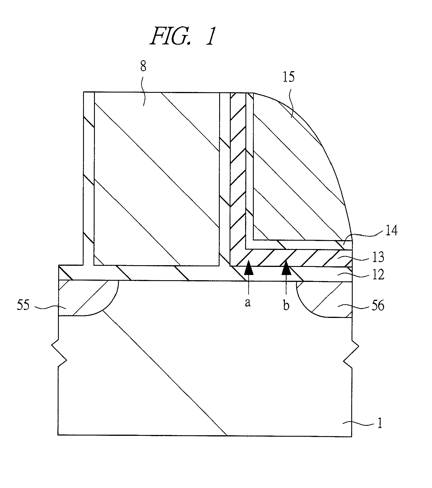
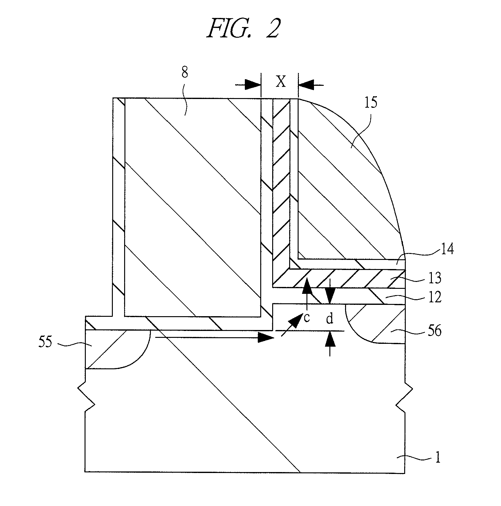
[0075]FIG. 4 is a plan view of a principal part illustrating a memory array region of a semiconductor device according to a first embodiment of the present invention, and FIG. 5 is a cross sectional view taken along the line A-A in FIG. 4. Note that, in FIG. 4, illustration of a part of members is omitted to easily see a constitution of the memory array region.

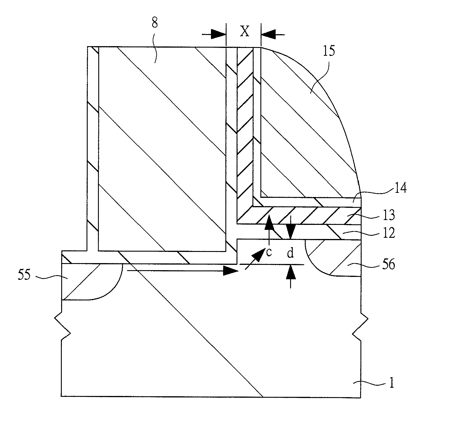
[0076]The semiconductor device according to the present embodiment includes a nonvolatile semiconductor storage device having a split-gate memory cell employing a MONOS type. The split-gate memory cell is composed of a select MOS transistor and a memory MOS transistor formed on a p-type well 3 on a p-type silicon substrate 1. A gate electrode (select gate 8) in the select MOS transistor is composed of an n-type polycrystalline silicon film and is formed on a gate insulating film 7 composed of a silicon dioxide film. A gate electrode (memory gate 15) in the memory MOS transistor is composed of an n-type polycrystalline silicon ...

second embodiment

[0098]FIG. 22 is a cross-sectional view of a principal part of a nonvolatile semiconductor storage device according to a second embodiment of the present invention. Hereinafter, a method of manufacturing the nonvolatile semiconductor storage device will be explained in an order of steps with reference to FIGS. 23 to 40.

[0099]First, as illustrated in FIG. 23, a surface of a silicon substrate 1 is etched by a well-known manufacturing technique with using a silicon nitride film 40 as a mask to form device-isolation trenches 2 on a main surface of the silicon substrate 1.

[0100]Next, as illustrated in FIG. 24, the silicon nitride film 40 is removed, and a p-type well 3 and an n-type well 4 are formed on the main surface of the silicon substrate 1. At this time, the device-isolation trenches 2 are not polished by a CMP (chemical mechanical polishing) method, and still remain. Next, the silicon substrate 1 is thermally oxidized, so that a gate insulating film 5 made of silicon dioxide havi...


PUM


Abstract

A step is provided between a substrate surface of a select gate and a substrate surface of a memory gate. When the substrate surface of the select gate is lower than the substrate surface of the memory gate, electrons in a channel upon writing obliquely flow in the step portion. Even if the electrons obtain the energy required for passing a barrier during the oblique flow, the electron injection does not occur because electrons are away from the substrate surface. The injection can occur only on a drain region side from a position where the electrons reach the substrate surface. As a result, the injection of the electrons into a gap region is suppressed, so that the electron distribution comes close to the hole distribution. Therefore, variation in a threshold value upon information retention is suppressed, and information-retaining characteristics of a memory cell are improved.

Description

CROSS-REFERENCE TO RELATED APPLICATION[0001]The present application claims priority from Japanese Patent Application No. JP 2009-003551 filed on Jan. 9, 2009, the content of which is hereby incorporated by reference into this application.TECHNICAL FIELD OF THE INVENTION[0002]The present invention relates to a semiconductor device and a method of manufacturing the same. More particularly, the present invention relates to a technique effectively applied to a semiconductor device having an electrically-rewritable nonvolatile memory and a method of manufacturing the same.BACKGROUND OF THE INVENTION[0003]A semiconductor device in which an electrically-rewritable nonvolatile memory and a microcomputer are mix mounted on a single silicon substrate is widely used in industrial machines, home electronics, vehicle-installed devices, and the like as an embedded microcomputer.[0004]The nonvolatile memory of the above-described semiconductor device stores programs required by the microcomputer, ...

Claims


Application Information

Patent Timeline
IPC IPC(8): H01L27/115H01L21/8246
CPCH01L21/28282H01L27/11568H01L27/11565H01L27/11529H01L29/40117H10B41/41H10B43/30H10B43/10
Inventor OKUYAMA, YUTAKAARIGANE, TSUYOSHI
Owner RENESAS ELECTRONICS CORP
Why Eureka
Try Eureka