

Process for producing multilayer printed wiring board
a multi-layer printed, wiring board technology, applied in the direction of layered products, chemistry apparatus and processes, other domestic articles, etc., can solve the problems of insufficient flowability of resin, interfering with the formation of insulating layer, and inability to afford flowability sufficient to cover circuit convexes and convexes on inner layer circuit boards, etc., to achieve superior mechanical strength, high productivity, and superior cover
- Summary
- Abstract
- Description
- Claims
- Application Information
AI Technical Summary
Benefits of technology
Problems solved by technology
Method used
Image

Examples
example 1
[0094]Liquid bisphenol A type epoxy resin (epoxy equivalents 180, “Epikote 828EL” manufactured by Japan Epoxy Resins Co., Ltd., 28 parts) and naphthalene type tetrafunctional epoxy resin (epoxy equivalents 163, “HP4700” manufactured by DIC Corporation, 28 parts) were dissolved in a mixed solution of methylethyl ketone (15 parts) and cyclohexanone (15 parts) with stirring while heating. Thereto were added a methylethyl ketone solution (110 parts) of a naphthol series curing agent (“SN-485” manufactured by Tohto Kasei Co., Ltd., phenolic hydroxyl group equivalents 215) having a solid content of 50%, a curing catalyst (“2E4MZ” manufactured by SHIKOKU CHEMICALS CORPORATION, 0.1 part), spherical silica (average particle size 0.5 μm, “SO-C2” manufactured by Admatechs Company Limited, 70 parts), and a polyvinyl butyral resin solution (“KS-1” manufactured by SEKISUI CHEMICAL CO., LTD., 30 parts, solid content 15%, 1:1 solution of ethanol:toluene), and the mixture was uniformly dispersed in ...
example 2
[0099]By an operation in the same manner as in Example 1 except that PET with a 38 μm-thick release layer (AL5 manufactured by Lintec Corporation: alkyd resin series release agent) described in Table 1 was used, evaluation was performed in the same manner as in Example 1.
example 3
Production of Multi-Layer Printed Wiring Board
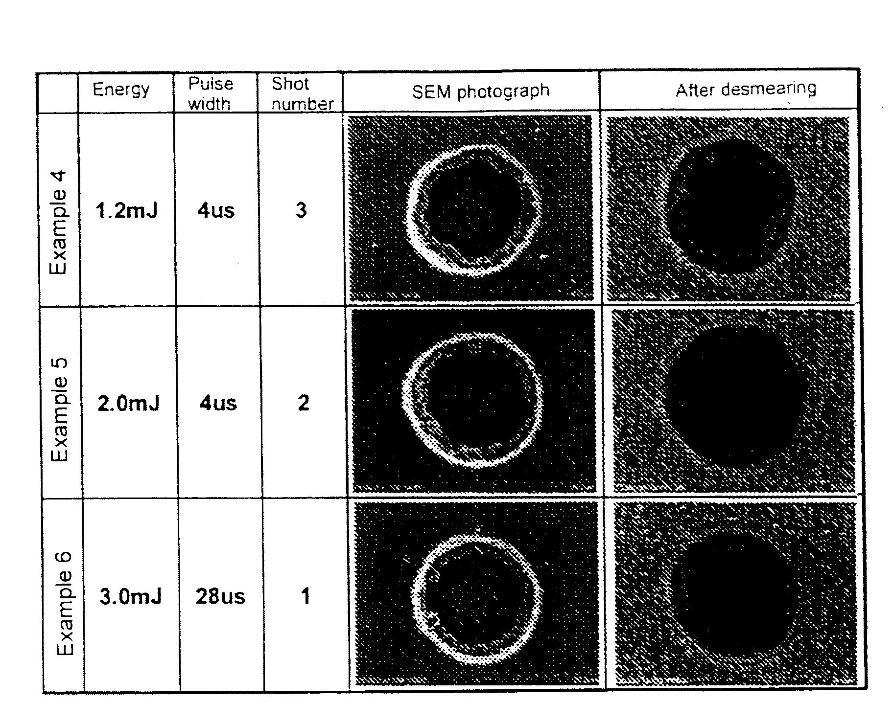
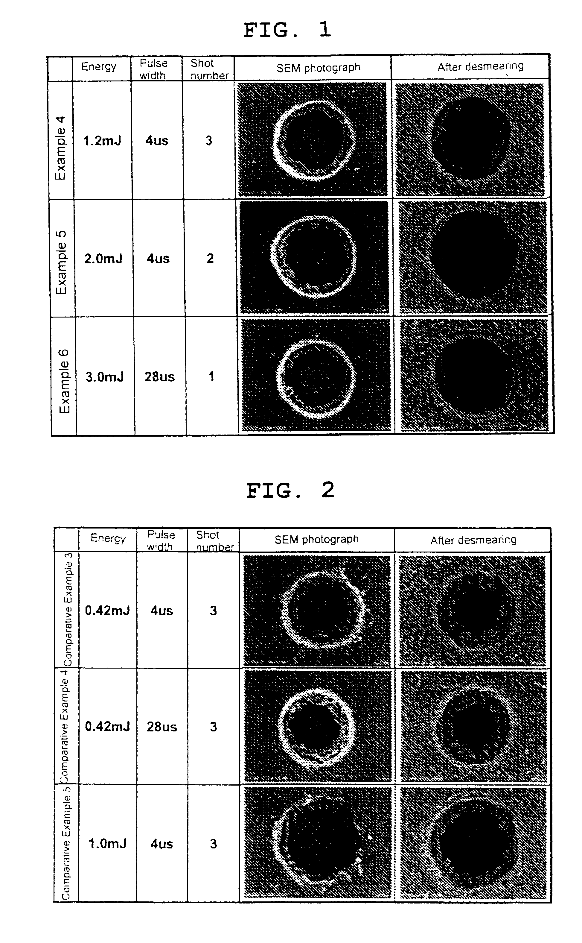
[0106]The substrate temporarily fit with a prepreg with a support film obtained in Example 2 was laminated on both surfaces by a vacuum laminating machine manufactured by MEIKI Co., Ltd. under the conditions of temperature 120° C., pressure 7 kgf / cm2, pressure 5 mmHg or below, and continuously subjected to a hot press with an SUS mirror panel under conditions of temperature 120° C., pressure 5 kgf / cm2. Then, the laminate with a release PET film was heated at 180° C. for 30 minutes to thermally cure the prepreg to form an insulating layer on both surfaces of the substrate. Thereafter, the release PET film was detached, and via hole was formed by laser drilling. For a surface treatment process of the insulating layer also serving as a desmear process, the following chemical solutions manufactured by Atotech Japan K.K. were used.
[0107]oxidant “Concentrate Compact CP” (alkaline permanganate solution)
[0108]reducing agent “Reduction solution S...
PUM
| Property | Measurement | Unit |
|---|---|---|
| Thickness | aaaaa | aaaaa |
| Thickness | aaaaa | aaaaa |
| Thickness | aaaaa | aaaaa |
Abstract
Description
Claims
Application Information