Light emitting device

Inactive Publication Date: 2010-08-26
DAI NIPPON PRINTING CO LTD
View PDF6 Cites 15 Cited by
  • Summary
  • Abstract
  • Description
  • Claims
  • Application Information

AI Technical Summary

Benefits of technology

[0017]According to the light emitting device of the present invention, a part of holes injected from the anode into the hole transport luminescent layer is recombined with electrons within the hole transport luminescent layer, and other holes which could not have contributed to the recombination are passed through the hole transport luminescent layer and are recombined with electrons within the electron transport layer at its portion close to the hol

Problems solved by technology

As shown in FIG. 1 in the document, the light emitting device is disadvantageous in that, since the luminescent layer provided in the light emitting device proposed in the document is formed of a monomolecular film of quantum dots, excitons generated by recombination of charges injected fr

Method used


Image

  • Light emitting device
  • Light emitting device
  • Light emitting device

Examples


Example

Example 1

[0083]A thin film (thickness: 150 nm) of indium tin oxide (ITO) was first formed by spattering on a glass substrate to form an anode. The substrate with the anode formed thereon was cleaned and was subjected to UV ozone treatment. Thereafter, a solution of polyethylenedioxythiophene-polystyrene sulfonic acid (abbreviated to “PEDOT-PSS”) was then spin coated in the air onto the ITO thin film, and the coating was dried to form a hole injection layer (thickness: 20 nm).

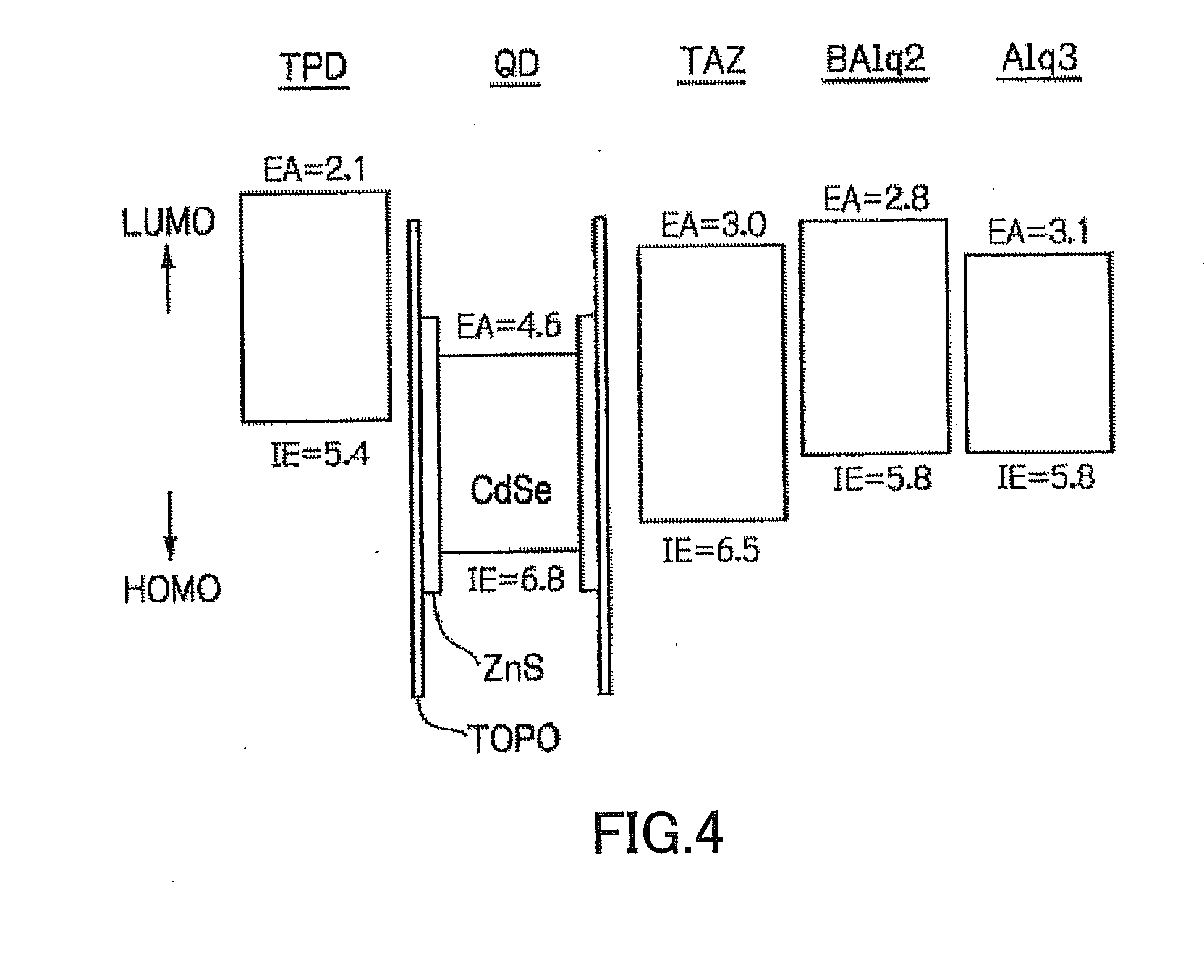
[0084]A mixed solution prepared by mixing N,N′-bis-(3-methylphenyl)-N,N′-bis-(phenyl)-benzidine (TPD) and quantum dots (core: CdSe; shell: ZnS; luminescence wavelength: 520 nm; manufactured by Evident Technologies, Inc.) with toluene was spin coated onto the hole injection layer within a glove box in a low-oxygen (oxygen concentration: not more than 0.1 ppm) and low-humidity (water vapor concentration: not more than 0.1 ppm) state to form a hole transport layer and a luminescent layer (total thickness: 40 nm). T...

Example

Comparative Example 1

[0087]A light emitting device of Comparative Example 1 was produced in the same manner as in Example 1, except that, instead of the electron transport layer formed of BAlq2, a 10-nm thick layer of TAZ (3-(4-biphenyl)-4-phenyl-5-t-butylphenyl-1,2,4-triazole) and a 40 nm-thick electron transport layer of Alq3 were formed in that order in vacuo (pressure: 5×10⁻⁵ Pa) by a resistance heating-type vapor deposition method.

Example

Comparative Example 2

[0088]A light emitting device of Comparative Example 2 was produced in the same manner as in Example 1, except that a 40 nm-thick electron transport layer of Alq3 was formed instead of the electron transport layer of BAlq2.


PUM


Abstract

The present invention provides a light emitting device that comprises a luminescent layer formed of a monomolecular film of quantum dots and has enhanced brightness and luminescence efficiency. A light emitting device 1 comprises at least an anode 3, a hole transport luminescent layer 5 formed of a material containing a hole transport material and quantum dots 11, an electron transport layer 7, and a cathode 4 provided in that order. The light emitting device 1 is constructed so that the hole mobility of the electron transport layer 7 is smaller than that of tris(8-quinolinolato)aluminum complex (Alq3), and, in the hole transport luminescent layer 5, excitons generated in the electron transport layer 7 migrate into the luminescent layer to emit light.

Description

CROSS-REFERENCE TO RELATED APPLICATIONS[0001]This application is based upon and claims the benefit of priority under Article 4 of the Paris Convention from the prior Japanese Patent Applications No. 256371 / 2007, filed on Sep. 28, 2007, the entire contents of the specifications, drawings, etc. of which are incorporated herein by reference.FIELD OF INVENTION[0002]The present invention relates to a light emitting device and more specifically relates to a light emitting device comprising an EL luminescent layer containing quantum dots.BACKGROUND ART[0003]An organic electroluminescence device (hereinafter referred to also as organic EL device) is a light emitting device having a laminate structure comprising an organic luminescent layer held between an anode and a cathode and is a self-luminous device utilizing luminescence attributable to recombination, within the luminescent layer, between holes injected from the anode and electrons injected from the cathode. The task of the organic EL...

Claims


Application Information

Patent Timeline
IPC IPC(8): H01L33/04H01L23/58
CPCB82Y20/00B82Y30/00C09K11/565C09K11/623H05B33/24H01L51/0081H01L51/5012H05B33/14C09K11/883H10K85/324H10K50/11H10K50/115
Inventor AKAI, TOMONORISHIMOGAWARA, MASAYA
Owner DAI NIPPON PRINTING CO LTD
Why Eureka
Try Eureka