Coupled Microstrip Lines with Tunable Characteristic Impedance and Wavelength

a microstrip line and characteristic impedance technology, applied in waveguides, conductive pattern formation, waveguide type devices, etc., can solve the problems of microstrip line ohmic losses becoming increasingly significant, occupying area, and forming ground plane drawbacks

Active Publication Date: 2010-08-26
TAIWAN SEMICON MFG CO LTD
View PDF26 Cites 46 Cited by
  • Summary
  • Abstract
  • Description
  • Claims
  • Application Information

AI Technical Summary

Benefits of technology

[0010]In accordance with another aspect of the present invention, a coupled microstrip line structure comprising a substrate, a first ground plane over the substrate, wherein the first ground plane is conductive and comprises a plurality of first ground strip shields substantially parallel to each other, and a first and second ground conductor electrically coupled to the plurality of first ground strip shields, wherein the first and second ground conductors are substantially parallel to each other is provided. The coupled microstrip line structure further comprises one or more dielectric layers over the first ground plane, a first signal line over the one or more dielectric layers, wherein the first signal line and the first ground conductor and the second ground conductor are substantially parallel, and a second signal line over the one or more dielectric layers, wherein the second signal line and the first ground conductor and the second ground conductor are substantially parallel, and wherein the second signal line is substantially parallel to the first signal line.
[0011]In accordance with yet another aspect of the present invention, a method of forming a coupled microstrip line structure, the method comprising providing a semiconductor substrate, forming a first ground plane over the semiconductor substrate, wherein the first ground plane comprises a plurality of first ground strip shields substantially parallel to each other, and forming a first ground conductor and a second ground conductor electrically coupled to the plurality of first ground strip shields, wherein the first and second ground conductors are substantially parallel to each other. The method further comprises forming one or more dielectric layers over the first ground plane, and forming a plurality of signal lines over the one or more dielectric layers.
[0012]The advantageous features of the present invention include adjustable characteristic impedances and adjustable characteristic wavelengths of coupled microstrip lines. The chip area required by the coupled microstrip line embodiments of the present invention is also reduced over conventional coupled microstrip lines.

Problems solved by technology

However, the formation of the ground plane also incurs drawbacks.
Consequently, ohmic losses in microstrip lines become increasingly more significant, and demand better impedance matching between microstrip lines and network devices.
Furthermore, the ground plane becomes a barrier for tuning the characteristic impedance of microstrip lines; this is due to the limited vertical distance between the signal line and the ground plane, a small distance with little room for tuning.
In addition, microstrip lines typically occupy a large chip area.
This is considered to be area-consuming.
With the increasing down-scaling of integrated circuits, the chip-area requirement of the microstrip lines becomes a bottleneck that prevents the integration of microwave devices and integrated circuits adopting CMOS devices.
Unfortunately, the microstrip line structure also has limited application in radio frequency (RF) circuits, particularly in microwave and millimeter wave integrated RF circuits like those in GPS satellite systems, PDA cell phones and ultra-wideband (UWB) wireless communication systems.
The parasitic loss of RF on-chip components cannot be scaled as readily as the parasitic loss that accompanies active devices such as transistors.

Method used


Image

  • Coupled Microstrip Lines with Tunable Characteristic Impedance and Wavelength
  • Coupled Microstrip Lines with Tunable Characteristic Impedance and Wavelength
  • Coupled Microstrip Lines with Tunable Characteristic Impedance and Wavelength

Examples


Embodiment Construction

[0022]The making and using of the presently illustrated embodiments are discussed in detail below. It should be appreciated, however, that the present invention provides many applicable inventive concepts that can be embodied in a wide variety of specific contexts. The specific embodiments discussed are merely illustrative of specific ways to make and use the invention, and do not limit the scope of the invention.

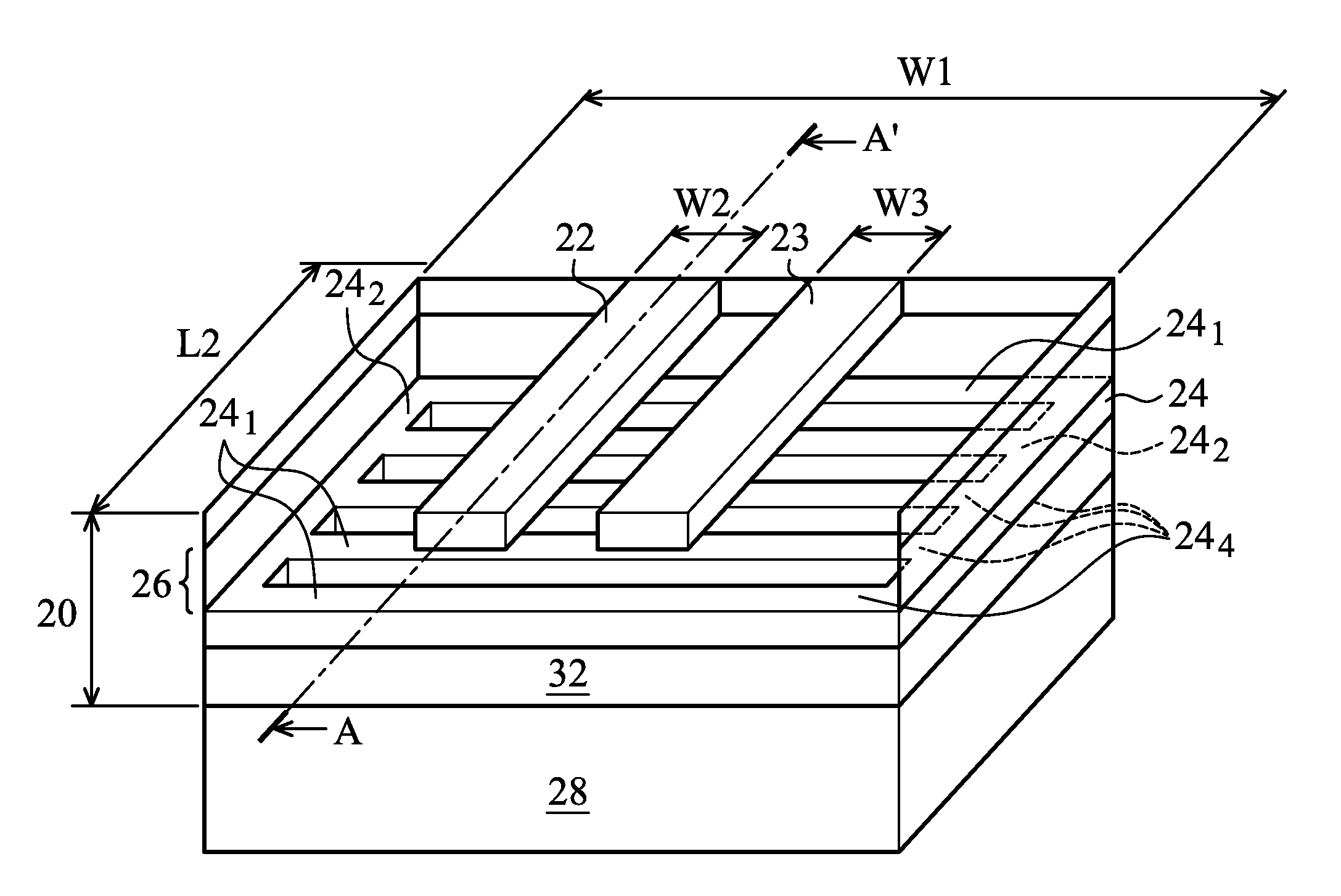
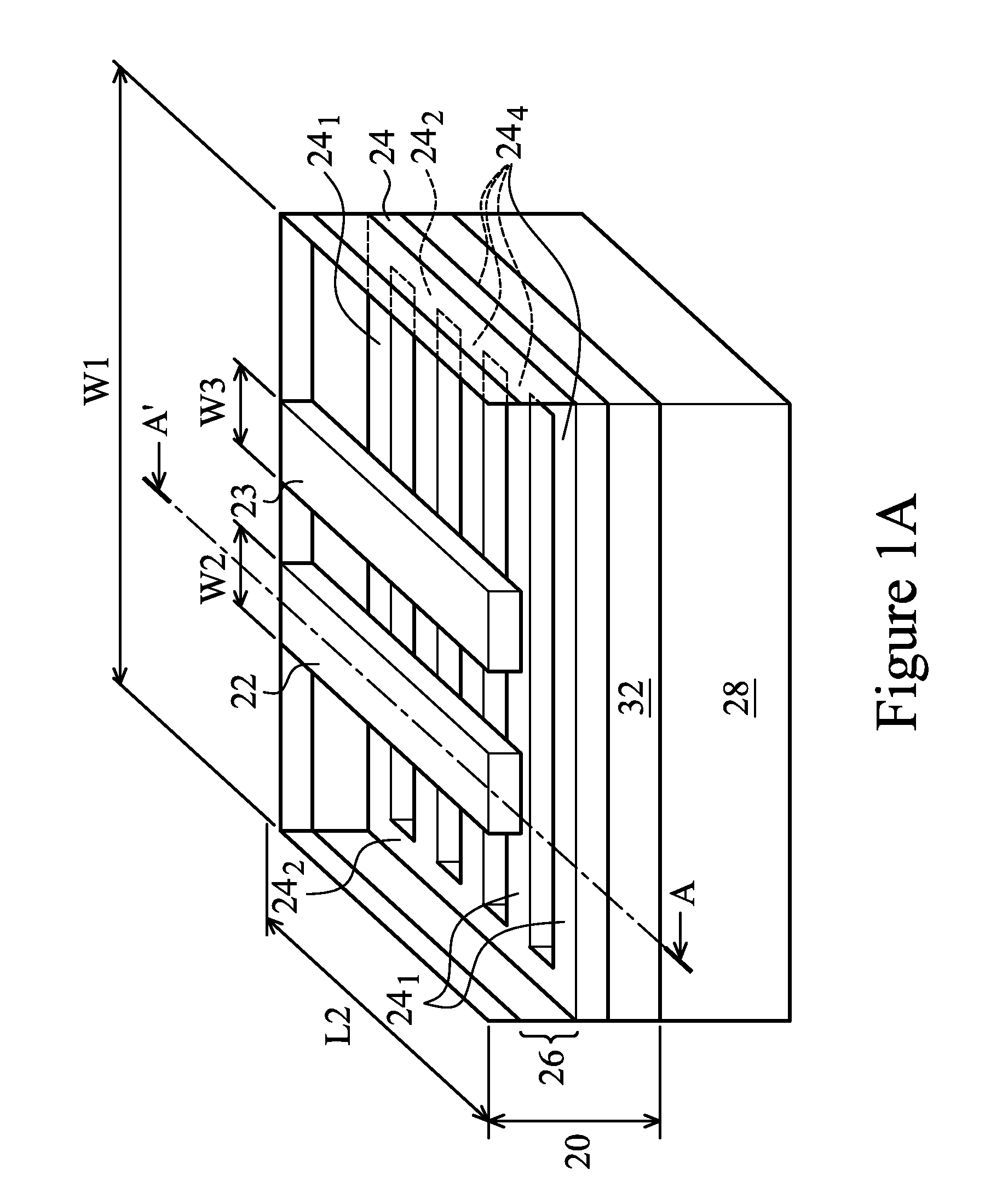
[0023]Novel coupled microstrip lines having tunable characteristic impedances and tunable characteristic wavelengths are provided. The variations of the illustrated embodiments are then discussed. Throughout the various views and illustrative embodiments of the present invention, like reference numbers are used to designate like elements.

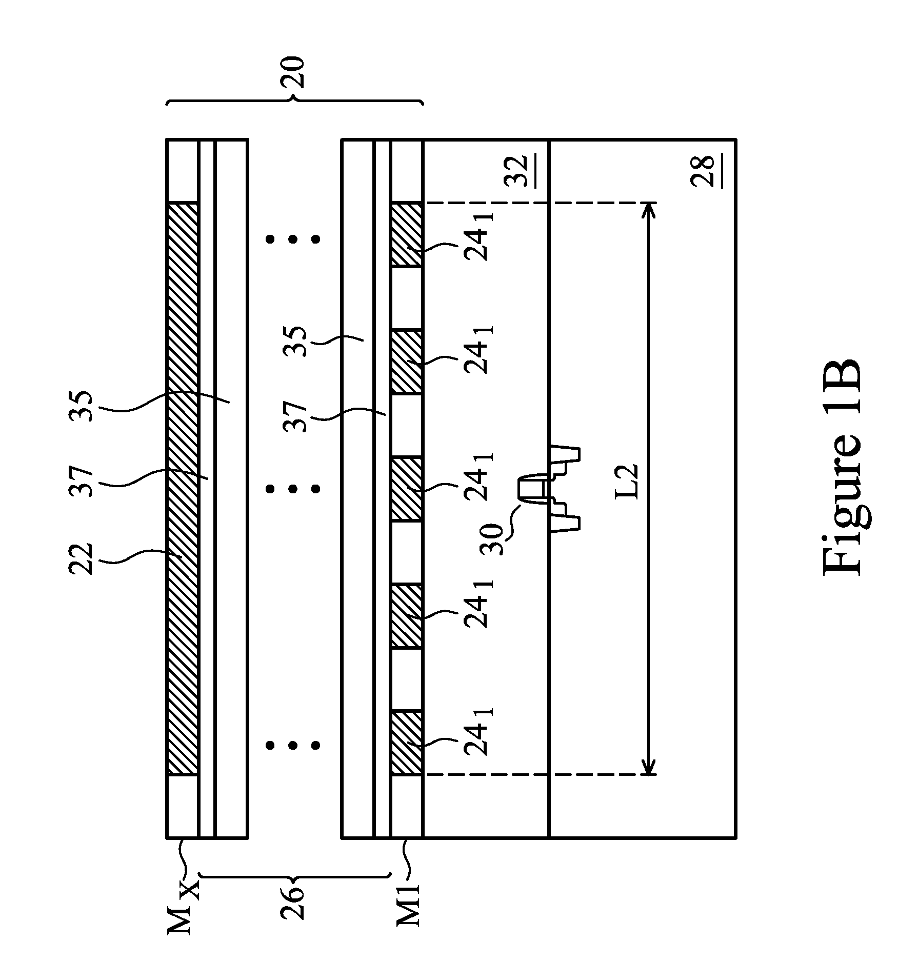
[0024]FIGS. 1A, 1B, and 1C illustrate a perspective view, a side view, and a top view, respectively, in accordance with an embodiment of the present invention, wherein the side view of FIG. 1B is a cross section taken along the A-A′ line of...


PUM

PropertyMeasurementUnit
lengthaaaaaaaaaa
electro-magnetic wavelengthaaaaaaaaaa
angleaaaaaaaaaa

Abstract

A coupled microstrip line structure having tunable characteristic impedance and wavelength are provided. In accordance with one aspect of the invention, a coupled microstrip line structure comprises a first ground plane having a plurality of first conductive strips separated by a dielectric material, and a first dielectric layer over the first ground plane. The coupled microstrip line further comprises a first signal line over the first dielectric layer, wherein the first signal line is directly above the plurality of first conductive strips, and wherein the first signal line and the plurality of first conductive strips are non-parallel, and a second signal line over the first dielectric layer, wherein the second signal line is directly above the plurality of first conductive strips, and wherein the second signal line and the plurality of first conductive strips are non-parallel, and wherein the second signal line is substantially parallel to the first signal line.

Description

[0001]This application claims the benefit of U.S. Provisional Application Ser. No. 61 / 155,411, filed on Feb. 25, 2009, entitled “Coupled Microstrip Lines with Tunable Characteristic Impedance and Wavelength,” which application is hereby incorporated herein by reference.TECHNICAL FIELD[0002]This invention relates generally to microstrip line structures and, more particularly, to coupled microstrip line structures having tunable characteristic impedances and tunable characteristic wavelengths.BACKGROUND[0003]Transmission lines are important elements in microwave circuit applications. These devices provide the interconnection between active and passive devices of microwave circuits, and are also utilized as impedance matching elements. A microstrip line is a type of transmission line widely utilized in monolithic microwave integrated circuit (MMIC) applications.[0004]Microstrip lines have a number of advantages when utilized in MMIC applications. First of all, since microstrip lines ar...

Claims


Application Information

Patent Timeline
Patent Type & Authority Applications(United States)
IPC IPC(8): H01P3/08H05K3/10
CPCH01L23/5225H01L23/66H01L2223/6627H01L2924/19032H01L2924/19051Y10T29/49155H01P3/08H01P5/185H01L2924/0002H01L2924/3011H01L2924/00
Inventor CHO, SHU-YING
Owner TAIWAN SEMICON MFG CO LTD
Why Eureka
Try Eureka