Semiconductor optoelectronic devices and methods for making semiconductor optoelectronic devices

a technology of optoelectronic devices and semiconductors, applied in photovoltaic energy generation, energy conversion devices, electrical apparatuses, etc., can solve problems such as degrading the overall quantum efficiency of devices

Inactive Publication Date: 2010-09-02
THE UNIV COURT OF THE UNIV OF GLASGOW
View PDF28 Cites 96 Cited by
  • Summary
  • Abstract
  • Description
  • Claims
  • Application Information

AI Technical Summary

Benefits of technology

[0073]As will be appreciated, this second aspect differs from the first aspect in that a window protection layer is not necessarily present in the final product (although such a layer may preferably be present). The etch stop layer is located in the contact region in the final product. During manufacture (at least), the etch stop layer is located above the window layer, but it is not essential for the etch stop layer to be present above the window layer in the final product (although this etch stop layer may be present in preferred embodiments). The advantage of using an etch stop layer in this way is that it may allow the contact material to be etched to an exact depth, which is advantageous in terms of leaving a known surface on which to deposit further layers, such as an anti-reflection coating(s).

Problems solved by technology

Charge carriers generated close to such a surface have a high probability of being captured and recombining non-radiatively, thereby degrading the overall quantum efficiency of the device.

Method used


Image

  • Semiconductor optoelectronic devices and methods for making semiconductor optoelectronic devices
  • Semiconductor optoelectronic devices and methods for making semiconductor optoelectronic devices
  • Semiconductor optoelectronic devices and methods for making semiconductor optoelectronic devices

Examples


Embodiment Construction

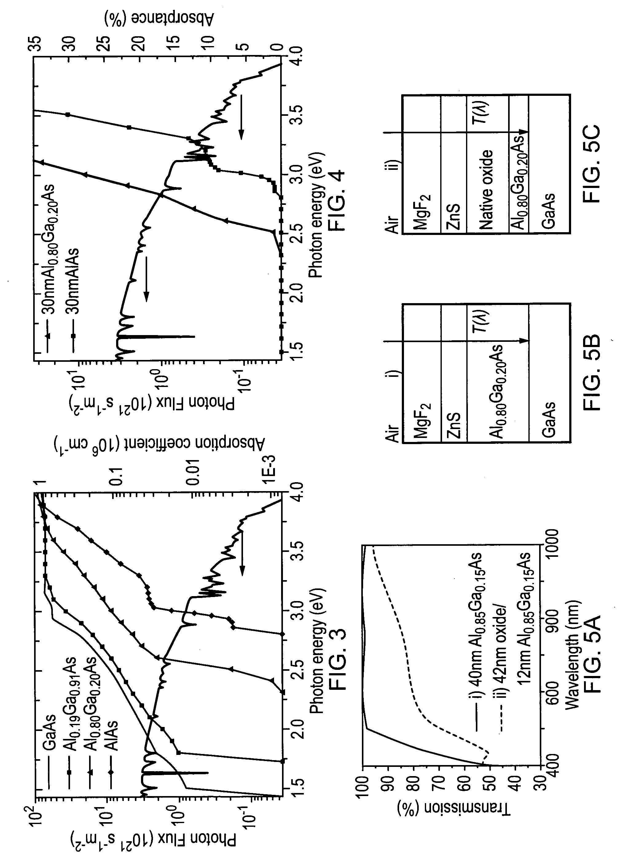
[0124]As explained above in relation to GaAs-based devices, in terms of the window performance, it is desirable to use a window layer having high aluminium fraction, but this is not generally advisable for practical reasons concerning oxidation / hydrolysis. The present inventors have devised devices and methods of fabrication in which it is possible to suppress exposure of the window layer to oxidizing species. In some preferred embodiments, this is done by ensuring that a protection layer (e.g. GaAs, (AlxGa1-x)0.51In0.49P, AlxGa1-xAs) is maintained to cover the window layer during and after the removal of the contact layer (also referred to herein as “cap layer”).

[0125]In one embodiment, the protection layer itself can be employed as the etch-stop layer in the selective etching process of the cap layer. Alternatively, in another embodiment, a dedicated etch-stop layer is introduced (between the protection layer and cap layer (contact layer)). This etch-stop layer assists in the sele...


PUM


Abstract

A semiconductor-based optoelectronic device such as a solar cell has an n-type layer and a p-type layer, together forming a p-n junction. Contact regions are formed on the device, with light-receiving regions between contact regions. A window layer is formed over the n-type layer or the p-type layer at the light-receiving region, the window layer promoting reduced carrier recombination at the surface of the n-type or p-type layer, and/or reflection of minority carriers in the n-type or p-type layer towards the p-n junction. The device has a window protection layer formed over the window layer, the window protection layer providing protection from degradation of the window layer during manufacture and/or operation of the device. For GaAs-based devices the window layer may be Al0.9Ga0.1As and the window protection layer may be GaAs. Additionally, an AlAs etch stop layer may be provided over the window protection layer.

Description

FIELD OF THE INVENTION[0001]The present invention relates to semiconductor optoelectronic devices and methods for making semiconductor optoelectronic devices. The invention is of particular, but not exclusive, interest to semiconductor photovoltaic devices.BACKGROUND TO THE INVENTION AND RELATED ART[0002]Semiconductor photovoltaic cells are known for use in renewable power generation, both for terrestrial and non-terrestrial applications.[0003]Many optoelectronic devices include a window layer, through which ‘useful photons’ travel, between light absorbing or light-emitting layers and the exterior of the opto-electronic device. These optoelectronic devices include, for example, photodiodes (including solar cells), phototransistors, light-emitting diodes, and vertical-cavity surface-emitting lasers.[0004]For a photodiode, it is possible to define ‘useful photons’ as those photons incident on the device that have photon energy, Ephoton=hf=hc / λ, within a certain range of energies that ...

Claims


Application Information

Patent Timeline
Patent Type & Authority Applications(United States)
IPC IPC(8): H01L27/142H01L31/0216H01L33/48H01L31/18H01L21/302H01L31/0693
CPCH01L31/02167H01L31/02168Y02E10/544H01L31/0693H01L31/03046Y02P70/50
Inventor FARMER, CORRIESTANLEY, COLIN
Owner THE UNIV COURT OF THE UNIV OF GLASGOW
Why Eureka
Try Eureka