Power converter and method for controlling power converter

a power converter and power converter technology, applied in the direction of electric variable regulation, process and machine control, instruments, etc., can solve the problems of reverse recovery, zvs is not possible in this control scheme, and the efficiency of the power converter is reduced, so as to avoid an increase in conduction loss, reduce loss, and large capacitance

Inactive Publication Date: 2010-09-02
FUJI ELECTRIC CO LTD
View PDF2 Cites 25 Cited by
  • Summary
  • Abstract
  • Description
  • Claims
  • Application Information

AI Technical Summary

Benefits of technology

[0039]The present invention makes it possible, without increasing the number of switching devices in a power converter, for the converter to keep the voltage change ratio (dv/dt) of the switching devices from exceeding a specified maximum value, thus avoiding an increase in conduction loss.
[0040]Moreover, the invention also makes it possible, in a DC/DC conversion circuit having a full-bridge configuration for large capacitance, to reduce loss associated with the charge

Problems solved by technology

However, ZVS is not possible in this control scheme.
Hence, when switching device S2 has turned on next, current readily flows to the body diode (not shown in FIG. 7) of the switching device S1, giving rise to the problem of reverse recovery.
Moreover, owing to loss at the interior of the MOSFET rises, the efficiency of the power converter decreases.
Hence, when reverse recovery arises, the loss increases.
This is because of the risk of MOSFET breakdown should the time change ratio exceed the specified maximum value.
When this happens, the voltage change ratio (dv/dt) of the body diode exceeds the specified maximum value and a parasitic bipolar transistor acts between the drain and the source, which may ultimately lead to breakdown of the body diode.
However, with either of these approaches, the power loss increases and the conversion efficiency decreases.
As a result, this method gives rise to a new problem; namely, an increase in the MOSFET conduc

Method used


Image

  • Power converter and method for controlling power converter
  • Power converter and method for controlling power converter
  • Power converter and method for controlling power converter

Examples


embodiment 1

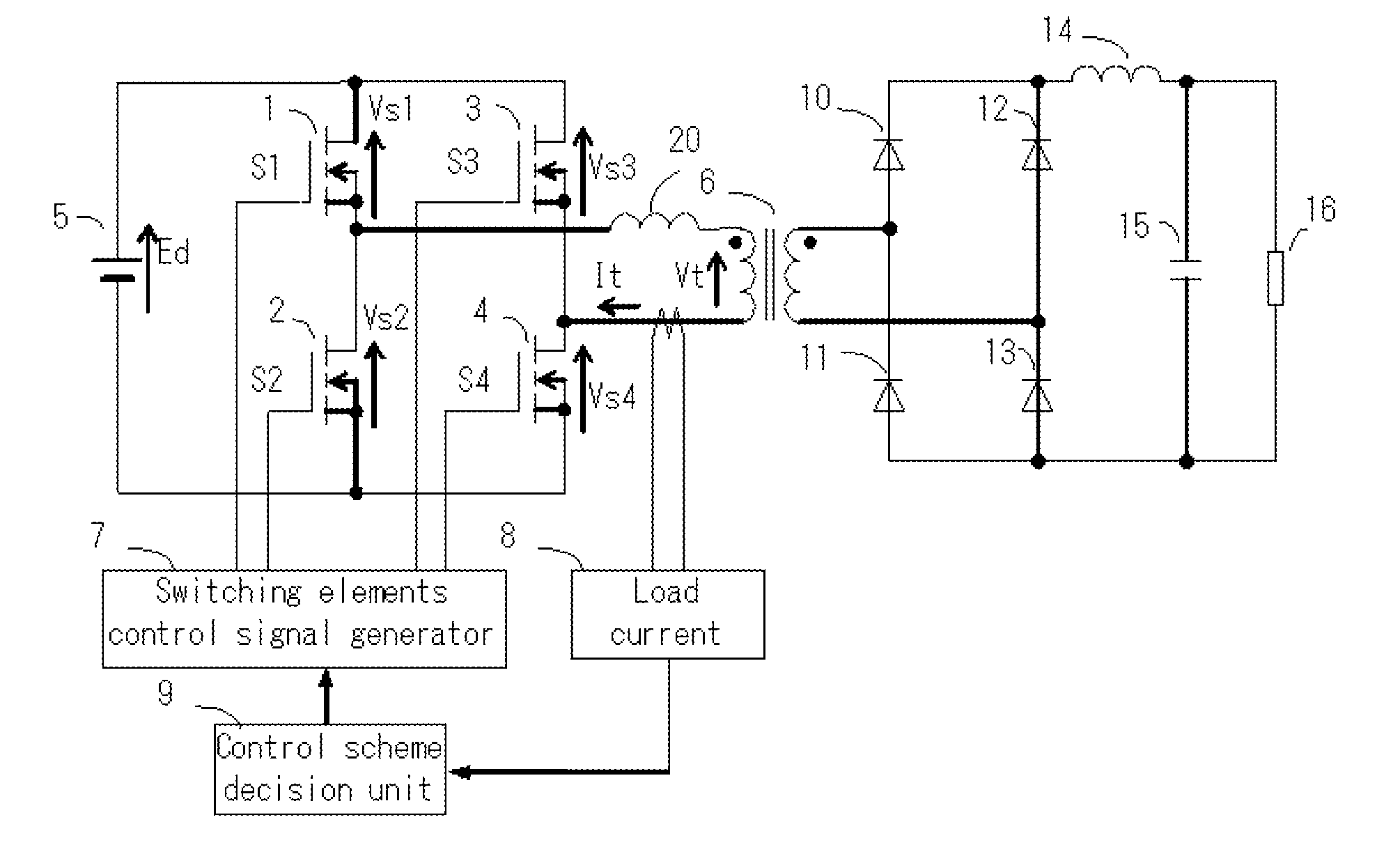
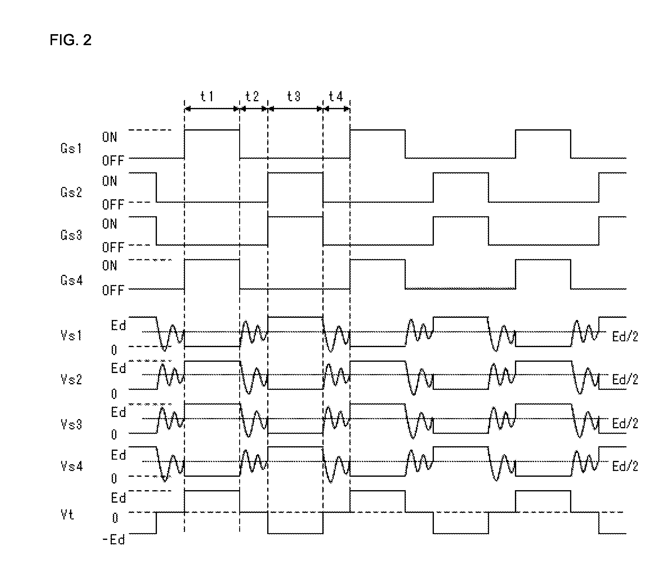
[0051]FIG. 1 is a circuit diagram illustrating a first embodiment of the present invention, and FIG. 2 is a chart of waveforms at various points for illustrating the operation of the same circuit.

[0052]In FIG. 1, elements having the same function as those in FIG. 7 showing a conventional power converter are denoted by the same reference symbols, and explanations of those elements are omitted. The first embodiment of the present invention differs from the power converter of FIG. 7 in that it is provided with a switching device control signal generator 7A and a control scheme decision unit 9.

[0053]GS1 to Gs4 in FIG. 2 are the gate driving voltage waveforms for switching devices S1 to S4 shown in FIG. 1, Vs1 to VS4 are the drain-source voltage waveforms for switching devices S1 to S4, and Vt is a primary winding voltage waveform for the transformer 6.

[0054]The switching devices S1 to S4 are driven by gate signals generated by the switching device control signal generator 7A. As a resul...

embodiment 2

[0064]FIG. 3 is a chart of waveforms at various points for illustrating a second embodiment according to the present invention. The circuit configuration is the same as in FIG. 7.

[0065]FIG. 3 shows an embodiment in which the times t2 and t4 when all the switching devices are off was regulated, and the switching devices were set so as to turn on when the switching device voltage had approached a minimum value. For example, the on timing of switching device 2 is regulated so that the switching device 2 turns on when the voltage Vs2 has approached a minimum value. However, if the positive side and negative side voltage time products applied to the transformer are not equal, the transformer magnetizes and excess current flows, damaging the circuit device. Hence, the on timing of switching device 2 must be regulated with condition t1=t3 being satisfied.

[0066]Accordingly, the sum of time t2 and time t4 is set constant and the ratio between times t2 and t4 is regulated. For example, if the...

embodiment 3

[0071]FIG. 4 shows a chart of operation waveforms corresponding to claim 4. In this Embodiment 3, the switching frequency is regulated in such a way that a switching device turns on when the voltage of the switching device approaches a minimum value. For example, when the switching frequency is made high, each of the times t0 to t5 becomes short; conversely, when the switching frequency is made low, each of the times t0 to t5 becomes long. However, the resonance period of the switching device voltage at times t2 and t4 when the switching devices are off is determined by the circuit constant or the parasitic component, and is fixed. Therefore, by regulating the switching frequency, it is possible to regulate the turn-on timing in such a way that the switching device turns on when the switching device voltage approaches a minimum value. As a result, actions and effects similar to those in Embodiment 2 are achieved.


PUM


Abstract

The invention prevents the voltage change ratio of switching devices of a power converter from exceeding a specified maximum rating, thus avoiding damage in switching devices and an increase in conduction loss. In a power converter having a plurality of switching devices, switching means for switching a control scheme for the switching devices to a phase shift control scheme or a pulse width modulation scheme is provided, whereby the control scheme for the switching devices is switched from the phase shift control scheme to the pulse width modulation scheme in a non-load or light-load state.

Description

BACKGROUND OF THE INVENTION[0001]The present invention relates to a power converter which achieves a higher efficiency and to a method for controlling such a power converter. More particularly, the invention relates to a converter suitable for use as an isolated DC / DC power converter and to a method for controlling such a power converter.[0002]FIG. 7 shows an example of an ordinary phase shift control scheme for the switching devices in a power converter. In the diagram, reference numbers 1 to 4 represent switching devices S1 to S4 composed of, e.g., metal oxide semiconductor field-effect transistors (MOSFET). Also shown in the diagram are a DC power supply 5, a transformer 6, a phase shift control signal generator 7, a load current detector 8, rectifier diodes 10 to 13, a smoothing inductor 14, a smoothing capacitor 15, and a load 16.[0003]FIG. 8 is a chart of the waveforms at various points for illustrating the operation of the power converter shown in FIG. 7. In this diagram, Gs1...

Claims


Application Information

Patent Timeline
IPC IPC(8): H02M3/335
CPCH02M1/32Y02B70/16H02M2001/0032H02M3/3376H02M1/0032H02M1/0058Y02B70/10
Inventor MINO, KAZUAKIITOH, KAZUNARI
Owner FUJI ELECTRIC CO LTD
Why Eureka
Try Eureka