
Semiconductor device

a technology of semiconductor devices and amplifiers, applied in the direction of rf amplifiers, basic electric elements, amplifier combinations, etc., can solve the problems of affecting the transmission affecting the body of a human being who makes use of mobile communication equipment, so as to improve the characteristic of the balance amplifier

Active Publication Date: 2010-09-09
MURATA MFG CO LTD
View PDF2 Cites 6 Cited by
  • Summary
  • Abstract
  • Description
  • Claims
  • Application Information

AI Technical Summary

Benefits of technology

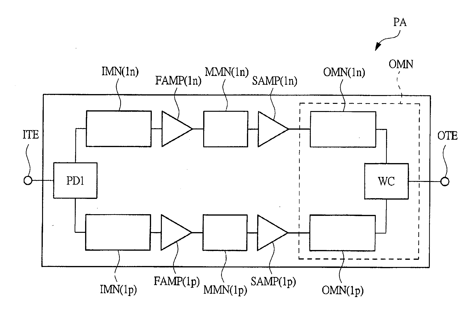
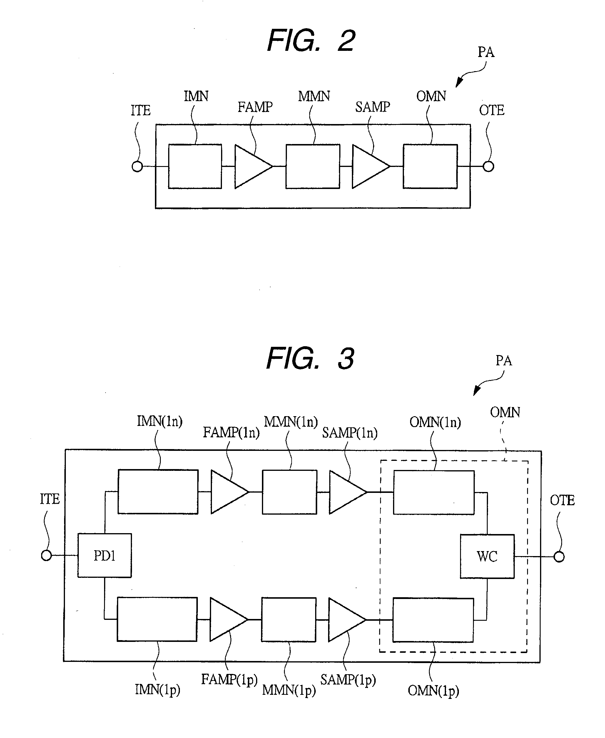
[0006]It has thus been examined by the present inventors et al. that the power amplifier is comprised of a balance amplifier to make it harder to affect the power of the transmit signal outputted from the power amplifier by the fluctuations in the load. The balance amplifier has two amplifying paths through which transmit signals having a phase difference of 90° with respect to each other are transmitted. Finally, the transmit signals transmitted over the two amplifying paths reach a single output by means of a power coupler. According to the balance amplifier, an advantage is brought about in that since the phases of the transmit signals transferred through the two amplifying paths are shifted by 90°, the output from the balance amplifier can be controlled approximately constant even though the load coupled to the output terminal of the balance amplifier fluctuates. Namely, in the balance amplifier, when one of the two amplifying paths changes to high impedance due to the fluctuations in the load, the other thereof changes to low impedance with respect to the fluctuations in the load. Therefore, when the transmit signals transferred through the two amplifying paths are combined together, the changes in the power of the transmit signals with respect to the fluctuations in the load can complement each other. As a result, the power of the transmit signal outputted from the balance amplifier can be kept approximately constant regardless of the fluctuations in the load. Thus, the power amplifier resistant to the fluctuations in the load can be configured by configuring the power amplifier from the balance amplifier.
[0008]An object of the present invention is to provide a technology capable of achieving an improvement in the characteristic of the balance amplifier when a power amplifier mounted to mobile communication equipment such as a cellular phone or the like is comprised of the balance amplifier.
[0013]A characteristic of a semiconductor device can be improved. Particularly when a power amplifier mounted onto mobile communication equipment such as a cellular phone or the like is comprised of a balance amplifier, an improvement in the characteristic of the balance amplifier can be achieved.

Problems solved by technology

The single amplifier is accompanied by a problem that a fluctuation in the transmit signal outputted from the single amplifier is liable to occur due to fluctuations in load coupled to the single amplifier.
When, for example, the power of the transmit signal outputted from the single amplifier becomes larger than a prescribed range due to the fluctuations in power, it adversely affects the body of a human being who makes use of mobile communication equipment.
On the other hand, when the power thereof becomes smaller than the prescribed range of the transmit signal outputted from the signal amplifier due to the power fluctuations, the transmission of the mobile communication equipment is interrupted.
In this case, when each low-band signal amplifying path and each high-band signal amplifying path perform signal transfer between wirings close to each other, the coupling capacitance between the wirings close to each other becomes large, so that crosstalk between the low-band and high-band signals becomes manifest as a problem.
Even when amplifying paths of a dual band-based power amplifier are respectively comprised of balance amplifiers, crosstalk between low-band and high-band signals becomes a problem.

Method used


Image

  • Semiconductor device
  • Semiconductor device
  • Semiconductor device

Examples


first embodiment

Configuration of Transceiver Section

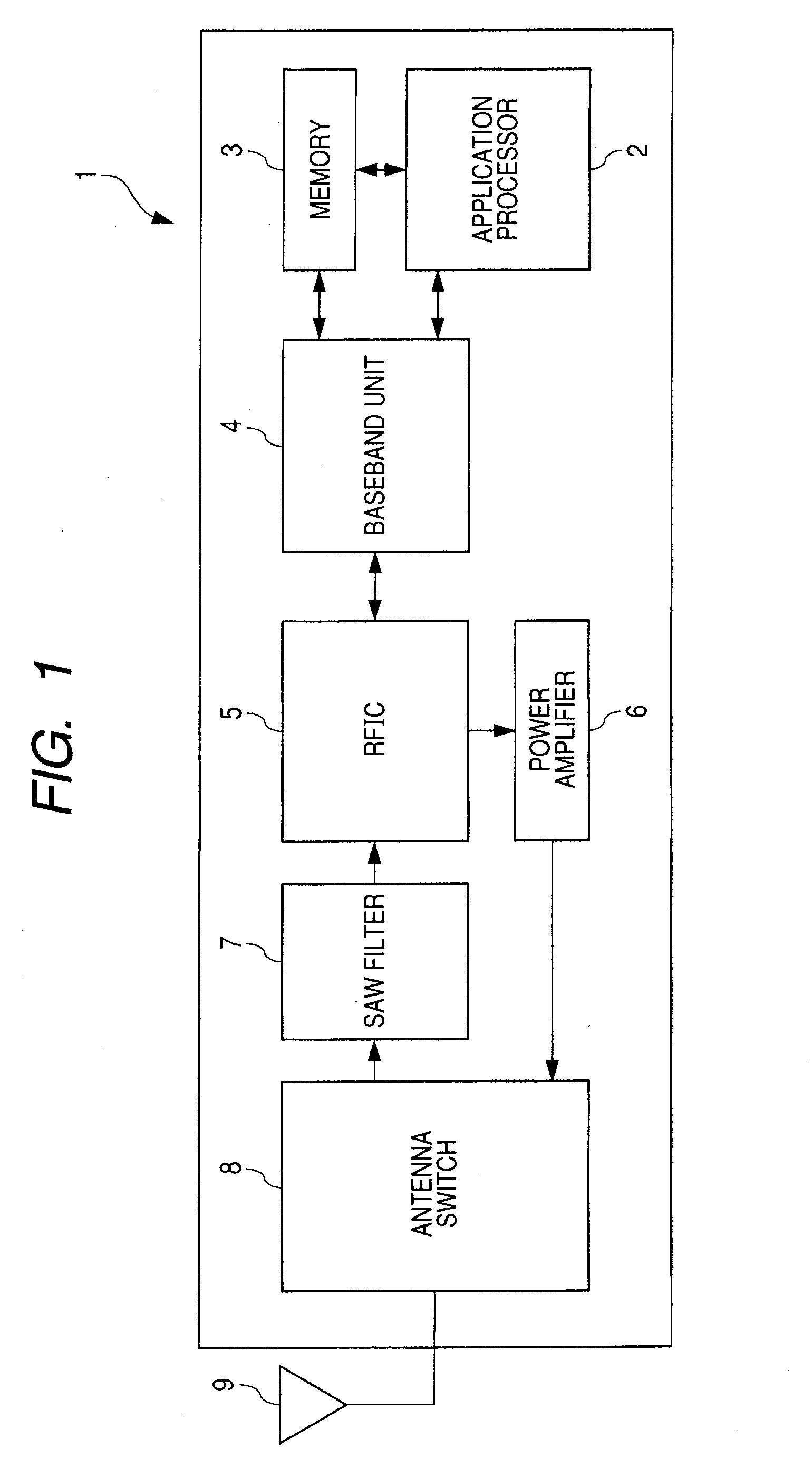
[0037]FIG. 1 is a block diagram showing a configuration of a transceiver section of a cellular phone. As shown in FIG. 1, the cellular phone 1 has an application processor 2, a memory 3, a baseband unit 4, an RFIC 5, a power amplifier 6, a SAW (Surface Acoustic Wave) filter 7, an antenna switch 8 and an antenna 9.

[0038]The application processor 2 comprises, for example, a CPU (Central Processing Unit) and has the function of realizing an application function of the cellular phone 1. Described concretely, the application processor 2 reads an instruction from the memory 3, decodes it and performs various arithmetic operations and control, based on the result of decoding thereby to realize the application function. The memory 3 has the function of storing data therein and stores therein, for example, a program for operating the application processor 2 and processing data at the application processor 2. Further, the memory 3 is capable of obtaining ac...

second embodiment

[0155]>

[0156]Although the first embodiment has explained the example in which the improvement in the characteristic of the balance amplifier is achieved by enhancing the symmetry between the passive parts mounted onto the wiring board WB, the present embodiment will explain an example in which a layout configuration lying within a semiconductor chip CHP is devised.

[0157]As shown in FIG. 8, the most part of the components of the low-band signal balance amplifier and the most part of the components of the high-band signal balance amplifier are formed within the semiconductor chip CHP. Accordingly, the layout thereof within the semiconductor chip CHP becomes important. A layout configuration example in which a low-band signal balance amplifier and a high-band signal balance amplifier are disposed on the sides opposite relative to a center line CL2 within a semiconductor chip CHP will be explained below.

[0158]FIG. 13 is a diagram showing a layout configuration within a semiconductor chi...


PUM


Abstract

The present invention provides a technology capable of achieving an improvement in the characteristic of a power amplifier when a power amplifier mounted onto mobile communication equipment such as a cellular phone is comprised of the balance amplifier. One feature of an embodiment resides in that each of passive parts disposed in a low-band signal negative path and each of passive parts disposed in a low-band signal positive path are placed in positions where they are symmetric with respect to a center line of a semiconductor chip. Thus, the symmetry between the low-band signal negative path and the low-band signal positive path is enhanced. As a result, a loss in matching due to the difference between the low-band signal negative path and the low-band signal positive path can be enough reduced, and the characteristic of a low-band signal balance amplifier can be enhanced.

Description

CROSS-REFERENCE TO RELATED APPLICATIONS[0001]The disclosure of Japanese Patent Application No. 2009-51203 filed on Mar. 4, 2009 including the specification, drawings and abstract is incorporated herein by reference in its entirety.BACKGROUND OF THE INVENTION[0002]The present invention relates to a semiconductor device, and particularly to a technology effective if applied to a semiconductor device used in mobile communication equipment such as a cellular phone.[0003]A configuration of a power amplifier for amplifying a transmit signal has been described in Japanese Unexamined Patent Publication No. 2008-135822 (patent document 1). The power amplifier described in the patent document 1 has two amplifying paths for transferring transmit signals having a phase difference of 90° with respect to each other. Namely, the power amplifier described in the patent document 1 is of a power amplifier which amplifies transmit signals having a phase difference of 90° respectively, and thereafter c...

Claims


Application Information

Patent Timeline
IPC IPC(8): H03F3/68
CPCH01L23/66H01L2924/1305H01L24/49H01L2223/6644H01L2223/6655H01L2224/05599H01L2224/49171H01L2224/85399H01L2924/01004H01L2924/01013H01L2924/01014H01L2924/01046H01L2924/01074H01L2924/14H01L2924/19041H01L2924/19042H01L2924/19105H01L2924/3011H03F1/56H03F3/195H03F3/211H03F3/245H03F3/68H03F2200/204H03F2200/222H03F2200/318H03F2200/387H03F2200/411H03F2200/451H03F2203/21142H01L24/06H01L2924/1306H01L2924/13064H01L2924/13091H01L2924/01041H01L2924/01033H01L2924/01006H01L2924/01005H01L2924/00014H01L2224/48227H01L24/48H01L2224/45099H01L2924/00H01L2224/05554H01L2924/30111
Inventor HAYATA, KANJIKURIYAMA, AKIRAHASE, MASATOSHIMATSUMOTO, HIDETOSHI
Owner MURATA MFG CO LTD
Learn More