Treatment system for flat substrates

a flat substrate and treatment system technology, applied in the direction of ion implantation coating, chemical vapor deposition coating, coating, etc., can solve the problems of high structural outlay, limited throughput, and large central handling device, so as to improve the production of flat substrates, reduce the number of process chambers, and reduce the cost of treatmen

US20100255196A1Inactive Publication Date: 2010-10-07LEYBOLD OPTICS
24 Cites 221 Cited by

Patent Information

Authority / Receiving Office
US · United States
Current Assignee / Owner
Publication Date
2010-10-07
Estimated Expiration
Not applicable · inactive patent

Smart Images

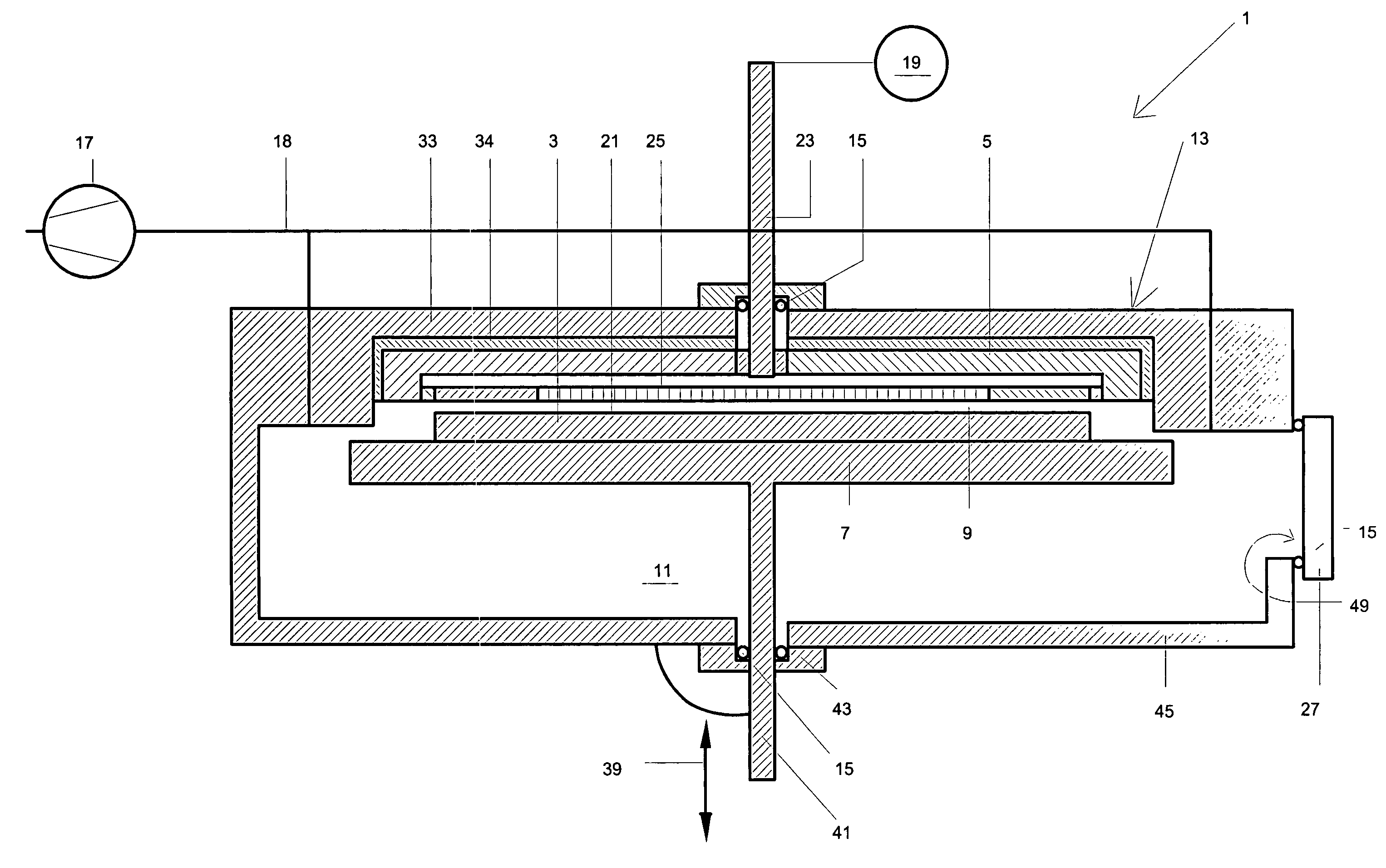
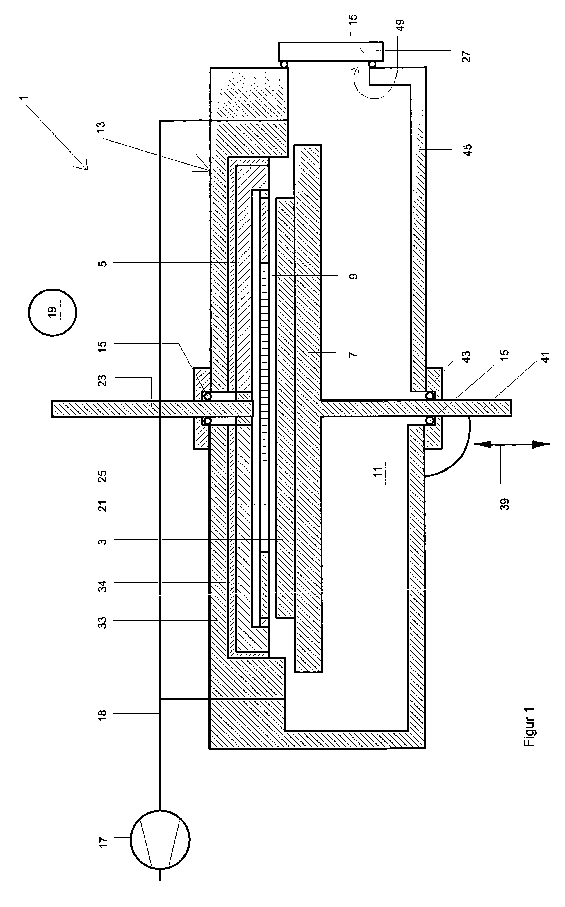
  • Figure 1
    Figure 1
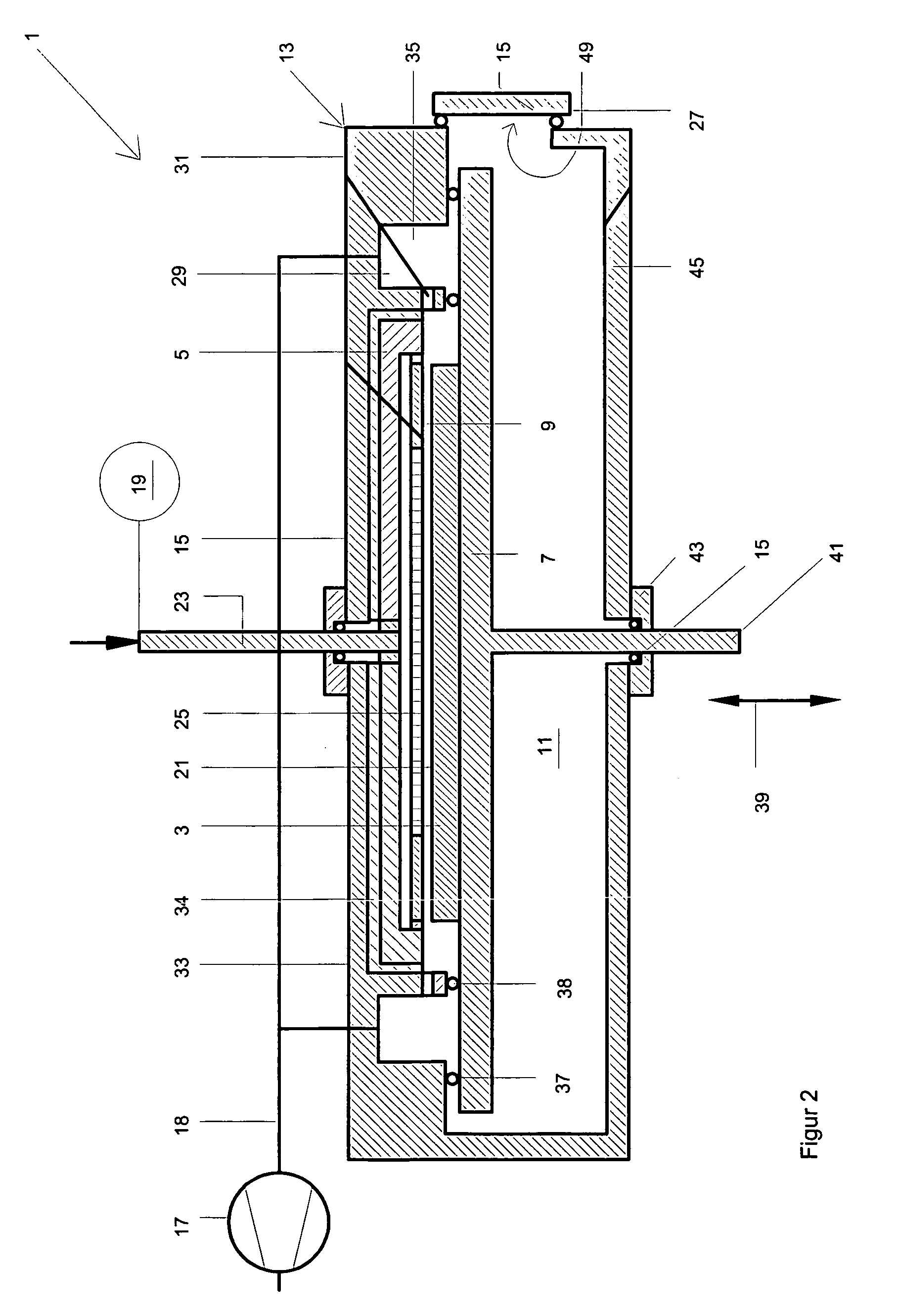
  • Figure 2
    Figure 2
  • Figure 3
    Figure 3
Patent Text Reader

Abstract

A reactor for the treatment of flat substrates includes a vacuum chamber with a process space arranged therein. A first electrode and a counterelectrode generate a plasma for the treatment of a surface to be treated and form two opposite walls of the process space. The reactor further includes means for introducing and means for removing gaseous material into and out from the process space. At least one substrate is accommodated by a front side of the counterelectrode. The vacuum chamber includes an opening having a closure device. The reactor includes a device for varying the relative distance between the first electrode and the counterelectrode and a device assigned to the counterelectrode for accommodating substrates. At least one substrate is arranged at an angle alpha in a range of between 0° and 90° relative to a perpendicular direction at least during the performance of the treatment.
Need to check novelty before this filing date? Find Prior Art

Description

TECHNICAL FIELD

[0001] The invention relates to treatment systems for substrates and, more particularly, to a reactor for treating flat substrates.BACKGROUND

[0002] EP 0312447 B1 has already disclosed a method for producing thin layers on substrates for electronic or optoelectronic use of one plasma deposition process (PECVD), wherein, in the presence of a deposition plasma, reaction gases for producing the layers are introduced into a plasma box arranged in a vacuum chamber. In this case, a pressure which is lower than that which prevails in the plasma box is generated and maintained in the vacuum chamber. Similar methods are also known from EP 02218112 B1 and U.S. Pat. No. 4,798,739. Further reactors, in particular comprising a plurality of chambers for the treatment of a substrate, are disclosed in DE 19901426 A1, U.S. Pat. No. 6,183,564 B1, U.S. Pat. No. 5,944,857, and also in the Japanese patent abstract JP 06267808 A.

[0003] The abovementioned PECVD method, which is used for the cos...

Examples

Embodiment Construction

[0026]The following explanation of reactors, handling, devices and methods for processing flat substrates will focus on structural aspects, where it is obvious to the person skilled in the art that these devices and methods are provided with sensors, heating and cooling units, control units and drives that are not specifically illustrated.

[0027]FIG. 1 shows, in a simplified illustration, a reactor 1 for the treatment of flat substrates 3. The reactor 1 can be designed as a PECVD reactor, for example. The reactor 1 comprises a process space 9 with an electrode 5 and a counterelectrode 7, which are designed for generating a plasma for the treatment of a surface to be treated of one or a plurality of flat substrates 3. The electrodes 5, 7 can be connected, or may have been connected, to a voltage source not illustrated in greater detail, preferably a radio-frequency supply source, in order to generate an electric field in the process space 9. The electrodes 5, 7 are preferably designed...