Method of manufacturing soi substrate

a technology of soi substrate and manufacturing method, which is applied in the direction of semiconductor/solid-state device manufacturing, basic electric elements, electric apparatus, etc., can solve the problems of adversely affecting the semiconductor properties, increase in oxygen defects, and significant deterioration of semiconductor properties, so as to reduce improve the properties of soi substrate and reduce the effect of oxygen defects or impurities

Inactive Publication Date: 2010-10-28
SEMICON ENERGY LAB CO LTD
View PDF41 Cites 26 Cited by
  • Summary
  • Abstract
  • Description
  • Claims
  • Application Information

AI Technical Summary

Benefits of technology

[0019]An embodiment of the disclosed invention enables formation of a reprocessed bond substrate with reduced oxygen defects or impurity elements, thereby improving the properties of an SOI substrate manufactured using this reprocessed bond substrate. Further, deterioration of the properties of a bond su...

Problems solved by technology

Repeated use of a bond substrate in this manner has involved a problem of an increase in oxygen defects such as an oxidation-induced stacking fault (OSF) due to an ion irradiation step, thermal history during split of the bond substrate, or the li...

Method used


Image

  • Method of manufacturing soi substrate
  • Method of manufacturing soi substrate
  • Method of manufacturing soi substrate

Examples


embodiment 1

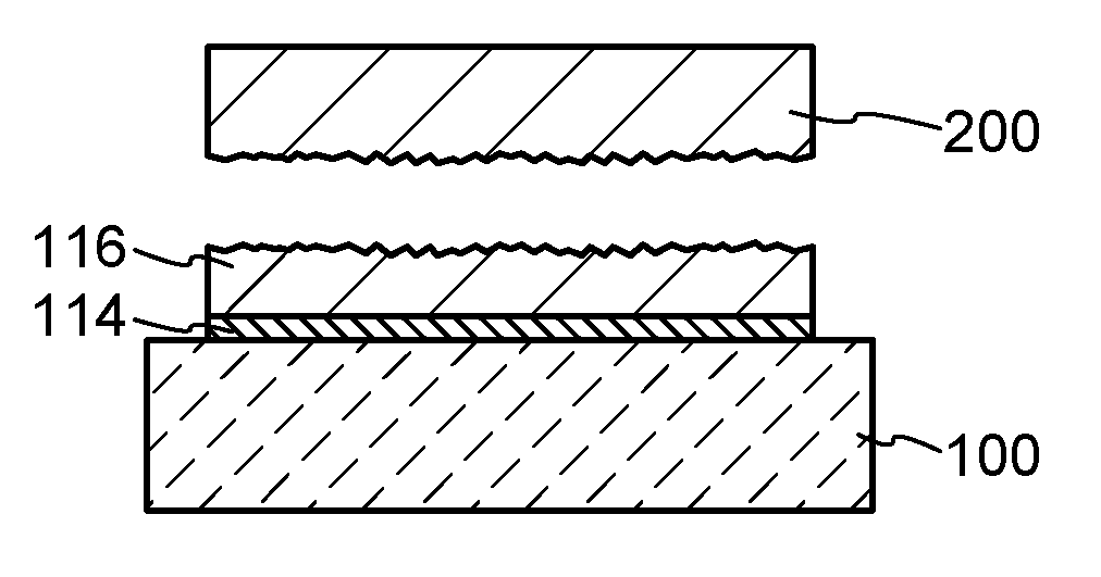
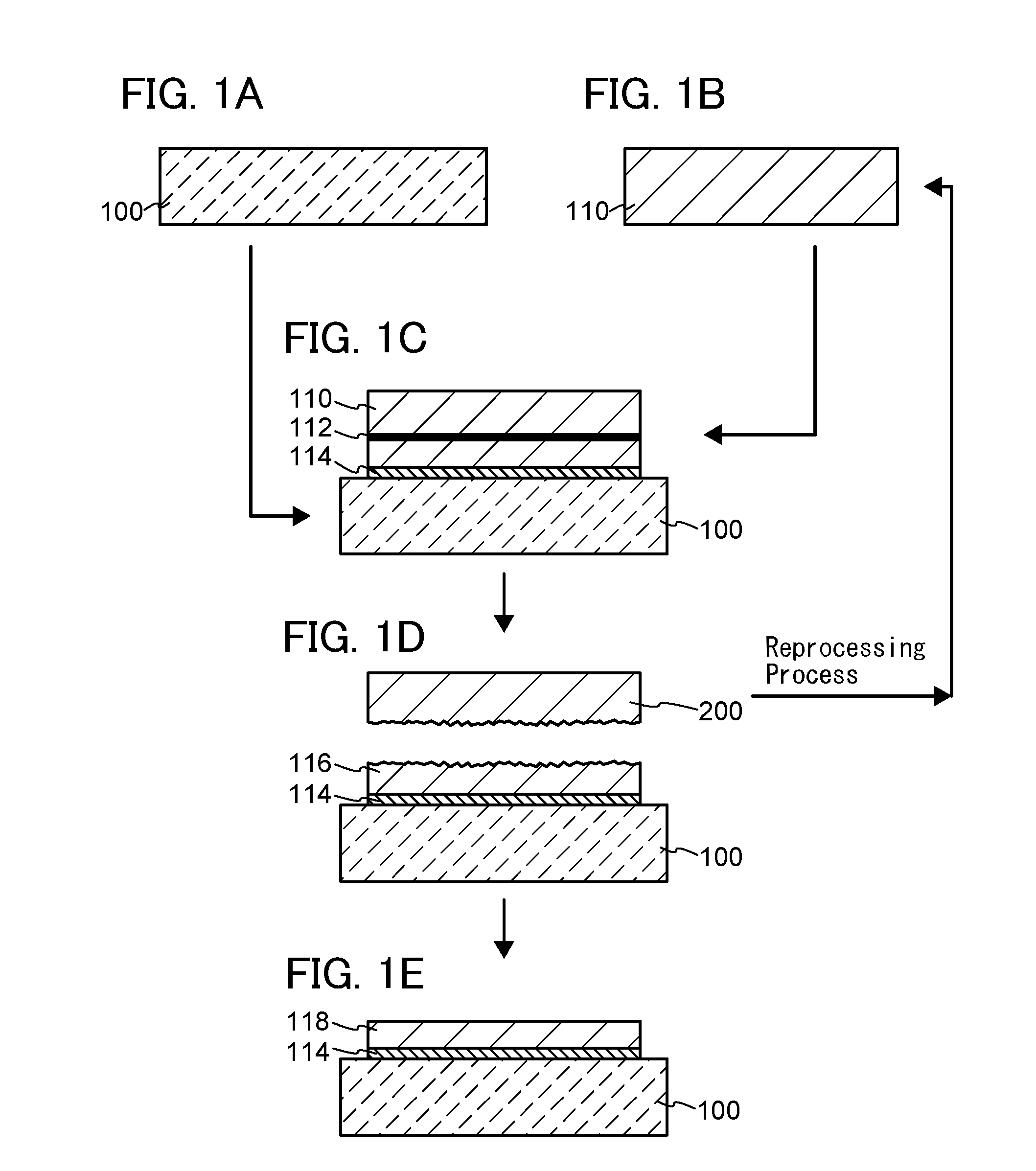
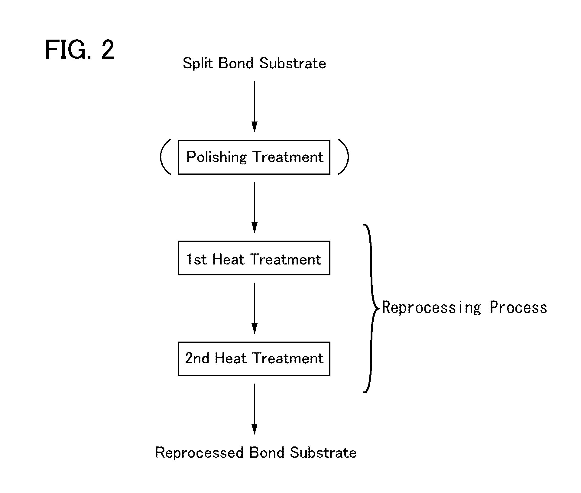
[0027]In this embodiment, an example of a method of manufacturing an SOI substrate is described with reference to drawings. Specifically, a process of manufacturing an SOI substrate is described using FIGS. 1A to 1E, and Process of Forming Reprocessed Bond Substrate is described using FIG. 2 and FIGS. 3A to 3E.

[0028]First, a base substrate 100 and a bond substrate 110 are prepared (see FIGS. 1A and 1B).

[0029]As the base substrate 100, a substrate formed of an insulator can be used. Specific examples thereof include a variety of glass substrates used in the electronics industry, such as substrates of aluminosilicate glass, aluminoborosilicate glass, and barium borosilicate glass, a quartz substrate, a ceramic substrate, and a sapphire substrate. Note that by containing a larger amount of barium oxide (BaO) than the amount of boric acid, a glass substrate as mentioned above has heat resistance such that it is more practicable. Thus, a glass substrate containing a larger amount of BaO ...

embodiment 2

[0064]In this embodiment, another example of the method of manufacturing an SOI substrates is described.

[0065]Although the process of reprocessing the split bond substrate is detailed in the above embodiment, an unused bond substrate may be subjected to this reprocessing process. In this case, removal of contaminants in the bond substrate and a reduction in defects are possible, contributing to a further improvement of the properties of a manufactured SOI substrate. Further, since the oxygen in the bond substrate is reduced and the DZ layer can be formed even to a certain depth of the bond substrate, growth of an OSF can be inhibited, and the number of times of repeated use of the bond substrate can be increased compared with a bond substrate that is not subjected to the process. Note that this process does not relate to the reprocess of the bond substrate and therefore can be simply called “heat treatment” or the like instead of “reprocessing process”.

[0066]Since the details of the...

embodiment 3

Process of Manufacturing SOI Substrate

[0071]In Embodiment 3, examples of the method of manufacturing an SOI substrate are described with reference to drawings. Note that parts that are different from those of the above Embodiments 1 and 2 are detailed while the descriptions of the same parts as those of Embodiment 1 and 2 are omitted.

[0072]To begin with, a manufacturing method according to First Mode is described with reference to FIGS. 4A to 4E.

[0073]First, the base substrate 100 is prepared (see FIG. 4A). As the base substrate 100, a light-transmitting glass substrate used for a liquid crystal display device or the like is available. As the glass substrate, a substrate having a strain point of 580° C. or more (preferably, 600° C. or more) may preferably be used. Further, the glass substrate is preferably a non-alkali glass substrate. The non-alkali glass substrate is formed using a glass material such as aluminosilicate glass, aluminoborosilicate glass, or barium borosilicate glas...


PUM


Abstract

The method of one embodiment of the present invention includes: a first step of irradiating a bond substrate with ions to form an embrittlement region in the bond substrate; a second step of bonding the bond substrate to a base substrate with an insulating layer therebetween; a third step of splitting the bond substrate at the embrittlement region to form a semiconductor layer over the base substrate with the insulating layer therebetween; and a fourth step of subjecting the bond substrate split at the embrittlement region to a first heat treatment in an argon atmosphere and then a second heat treatment in an atmosphere of a mixture of oxygen and nitrogen to form a reprocessed bond substrate. The reprocessed bond substrate is used again as a bond substrate in the first step.

Description

BACKGROUND OF THE INVENTION[0001]1. Field of the Invention[0002]The present invention relates to a method of manufacturing a substrate over which a semiconductor layer is provided with an insulating layer therebetween, and particularly relates to a method of manufacturing a silicon on insulator (SOI) substrate. Further, the present invention relates to a method of recycling a bond substrate in the manufacturing method of an SOI substrate.[0003]2. Description of the Related Art[0004]As substrates suitable for manufacture of semiconductor devices that achieve low power consumption and high-speed operation, attention has been directed to SOI substrates in which a semiconductor layer is provided over a base substrate having an insulating surface.[0005]One of known methods of manufacturing an SOI substrate is a hydrogen ion implantation separation method (see Patent Document 1). The hydrogen ion implantation separation method is a technique of forming an SOI substrate in the following ma...

Claims


Application Information

Patent Timeline
IPC IPC(8): H01L21/762
CPCH01L21/76254H01L21/02488H01L27/1203
Inventor HANAOKA, KAZUYATSUYA, HIDEKINAGAI, MASAHARU
Owner SEMICON ENERGY LAB CO LTD
Why Eureka
Try Eureka