Semiconductor integrated optical device and method of making the same

a technology of integrated optical devices and semiconductors, applied in the direction of optical elements, semiconductor lasers, instruments, etc., can solve the problems of inability to achieve high yield rates of integrated optical circuits, and achieve the effect of enhancing lithographic accuracy and being ready to mak

Inactive Publication Date: 2010-11-11
SUMITOMO ELECTRIC IND LTD
View PDF11 Cites 21 Cited by
  • Summary
  • Abstract
  • Description
  • Claims
  • Application Information

AI Technical Summary

Benefits of technology

[0012]Such a configuration enables precise alignment of the first optical waveguide with the second optical waveguide. The vertical positions of these optical waveguides can be adjusted accurately through control of thickness of the silicon oxide layer and semiconductor layers. The thickness of each layer is controlled accurately by determination of the time of deposition. The horizontal positions of these optical waveguides can be adjusted accurately through photolithographic formation of the first and second optical waveguides. Thus, the semiconductor integrated optical device of the present invention can exhibit an enhanced coupling efficiency between the semiconductor optical device region and the optical waveguide region.
[0022]The silicon oxide layer may have a compressive internal stress in a range of 50 MPa to 500 MPa. In cases where the internal stress in the silicon oxide layer is a compressive stress greater than or equal to 50 MPa, flaking and cracking of the silicon oxide layer can be suppressed even if the silicon oxide layer is relatively thick, for example, greater than or equal to 2 μm thick. In cases where the internal stress in the silicon oxide layer is a compressive stress not greater than 500 MPa, a warp of the group III-V compound semiconductor substrate can be suppressed to enhance lithographic accuracy in a post-process.

Problems solved by technology

As a result, the yield rate of producing integrated optical circuits is inevitably low.

Method used


Image

  • Semiconductor integrated optical device and method of making the same
  • Semiconductor integrated optical device and method of making the same
  • Semiconductor integrated optical device and method of making the same

Examples


first embodiment

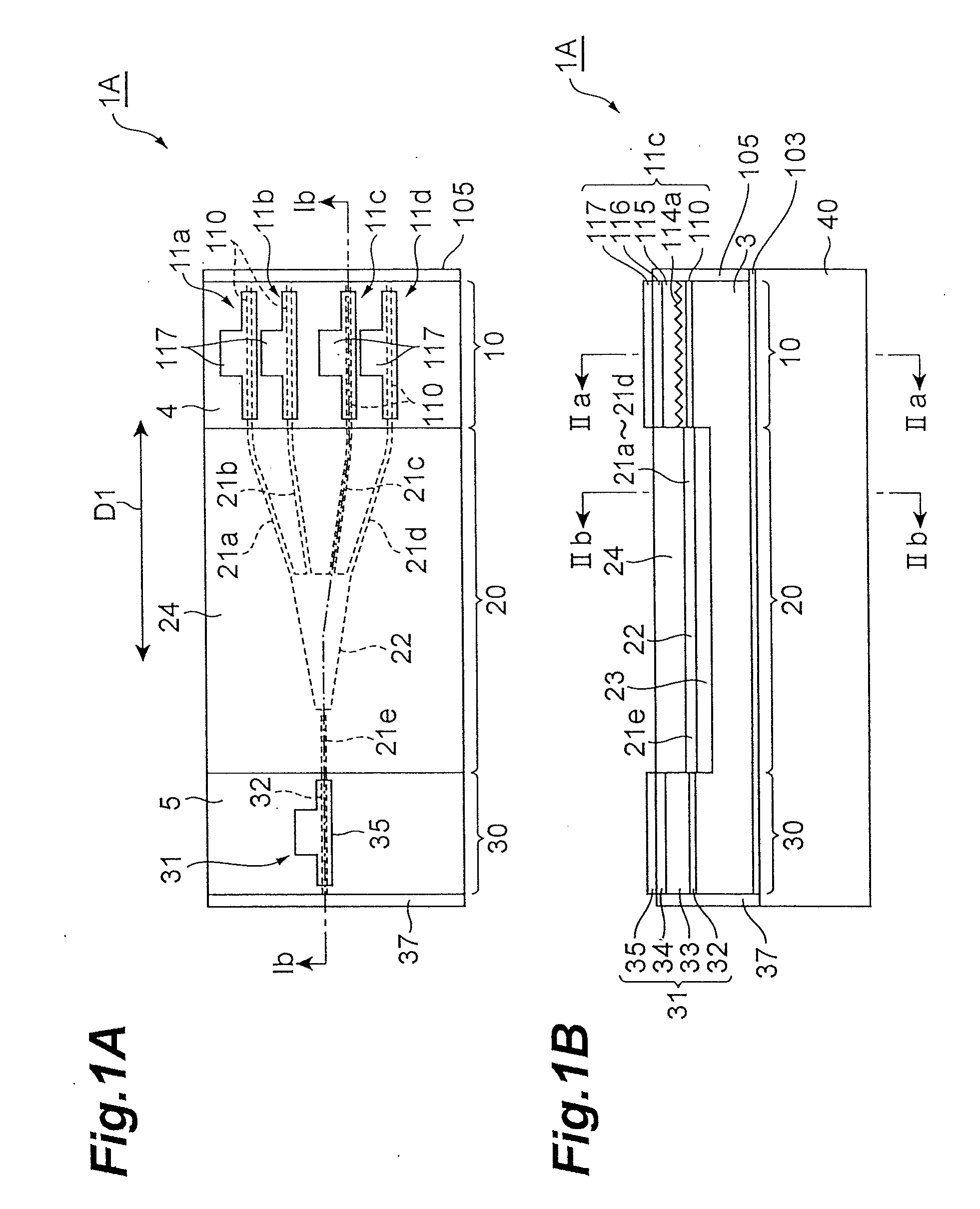
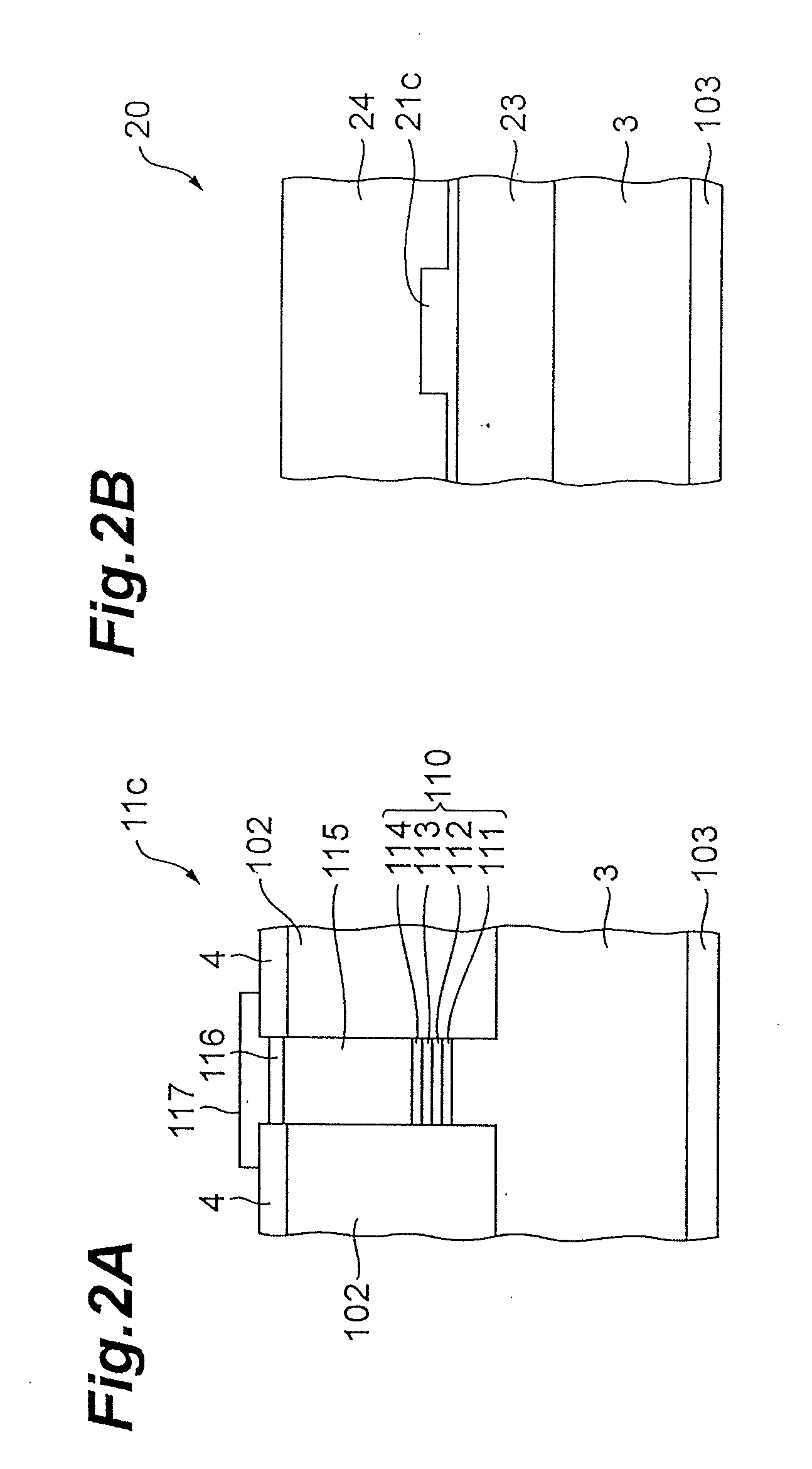
[0051]FIG. 1A is a plan view of a semiconductor integrated optical device in the present invention. FIG. 1B is a cross-sectional view taken along the line Ib-Ib in FIG. 1A. The semiconductor integrated optical device 1A illustrated in FIGS. 1A and 1B comprises a semiconductor laser region 10, an optical waveguide region 20, and a light amplification region 30. The semiconductor laser region 10 has a plurality of DFB semiconductor lasers 11a to 11d. The optical waveguide region 20 has a plurality of optical waveguides 21a to 21e and a multi-mode interferometer (MMI) wavelength multi / demultiplexer 22 (hereinafter referred to as MMI coupler). The light amplification region 30 has a semiconductor optical amplifier (SOA) 31. The semiconductor laser region 10 and the light amplification region 30 are provided for semiconductor optical device regions in the present embodiment.

[0052]As illustrated in FIG. 1B, a semiconductor laser region 10, an optical waveguide region 20, and a light ampli...

second embodiment

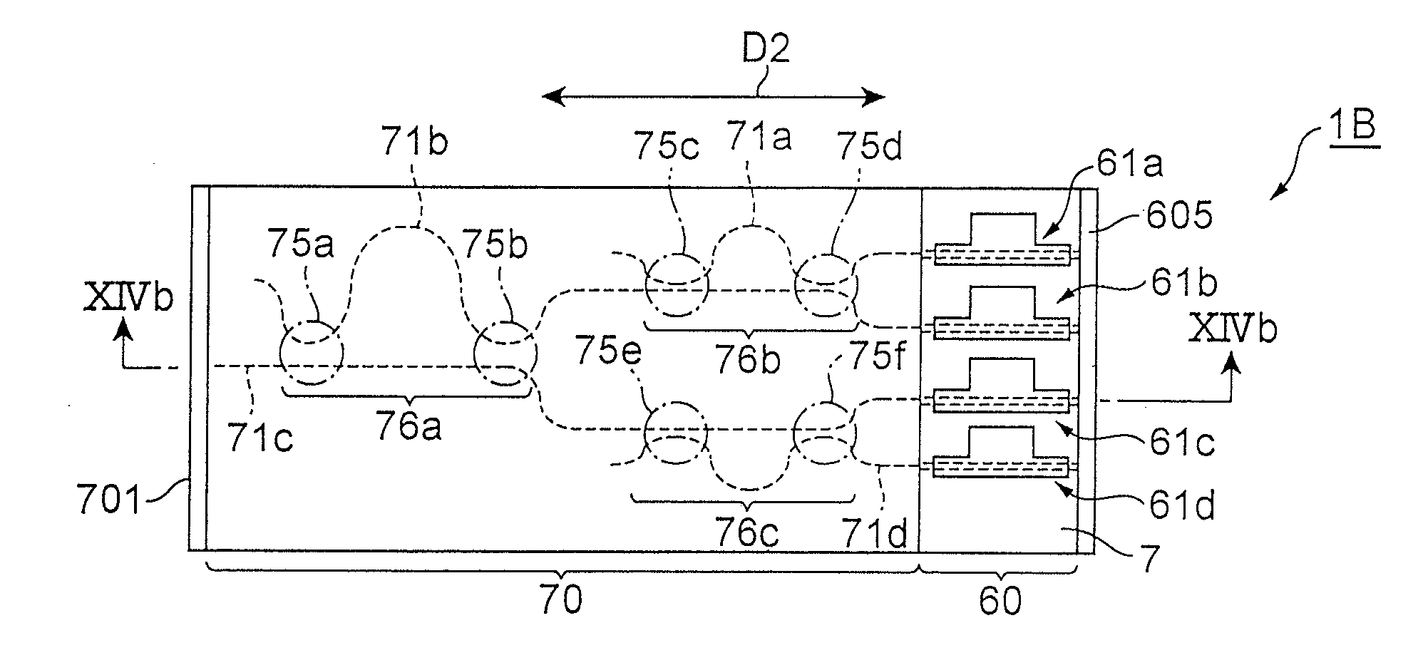
[0095]FIG. 14A is a plan view of a semiconductor integrated optical device in the present invention. FIG. 14B is a cross-sectional view taken along the line XIVb-XIVb in FIG. 14A. As shown in FIGS. 14A and 14B, the semiconductor integrated optical device 1B comprises a photodiode region 60 and an optical waveguide region 70. The photodiode region 60 has photodiode structures 61a to 61d. The optical waveguide region 70 has optical waveguides 71a to 71d. The photodiode region 60 is provided for a semiconductor optical device region of the present embodiment. As shown in FIG. 14B, the photodiode region 60 and the optical waveguide region 70 are formed on a semiconductor substrate 6. The photodiode region 60 and the optical waveguide region 70 are arranged in a predetermined direction D2. The semiconductor substrate 6 can be a group III-V compound semiconductor substrate in the present embodiment. The semiconductor substrate 6 is composed of first conductive type semiconductor such as n...


PUM


Abstract

A semiconductor integrated optical device includes a group III-V compound semiconductor substrate, a semiconductor optical device region, and an optical waveguide region. The semiconductor optical device region and the optical waveguide region are arranged on the group III-V compound semiconductor substrate. The semiconductor optical device region has a first optical waveguide made of group III-V compound semiconductor. The optical waveguide region has a second optical waveguide optically coupled with the first optical waveguide. The optical waveguide region further includes a silicon oxide layer. The silicon oxide layer is disposed between the group III-V compound semiconductor substrate and the second optical waveguide. The second optical waveguide is made of semiconductor which is different from the group III-V compound semiconductor.

Description

BACKGROUND OF THE INVENTION[0001]1. Field of the Invention[0002]The present invention relates to a semiconductor integrated optical device and a method of making the same.[0003]2. Related Background Art[0004]Japanese Unexamined Patent Application Publication No. 2007-164110 (hereinafter, referred to as “Patent Document 1”) discloses an integrated optical circuit in which a light emitting device or a light receiving device is mounted on a silicon substrate having an optical waveguide. According to this Patent Document 1, a method referred to as “epitaxial lift-off” is used for making the integrated optical circuit. This method includes steps of growing semiconductor layers on a wafer to make an optical device including the light emitting device or the light receiving device, protecting the optical device with a waxing compound, cutting the wafer to fowl the optical device chip, and arranging the optical device onto the silicon wafer having the optical waveguide.[0005]Alexander W. Fan...

Claims


Application Information

Patent Timeline
Patent Type & Authority Applications(United States)
IPC IPC(8): G01B9/02G02B6/12H01L21/20H01S5/125G02B6/26
CPCB82Y20/00G01B9/02G02B6/12007G02B6/125G02B6/132G02B6/136H01S5/50G02B6/29355G02B2006/12078H01S5/02248H01S5/2275H01S5/34306H01S5/4031G02B6/2813H01S5/02325
Inventor FUKUDA, CHIE
Owner SUMITOMO ELECTRIC IND LTD
Why Eureka
Try Eureka