Conductive bump structure for semiconductor device and fabrication method thereof

a technology of conductive bumps and semiconductor devices, which is applied in the direction of semiconductor devices, basic electric elements, electrical apparatus, etc., can solve the problems of bump cracking, easy cracking of solder bumps, and poor prior art fabricated structure of common solder bumps, etc., to achieve simple and low-cost fabrication processes, increase the bonding area of solder materials, and reduce the effect of bump cracking

Inactive Publication Date: 2010-11-25
SILICONWARE PRECISION IND CO LTD
View PDF5 Cites 10 Cited by
  • Summary
  • Abstract
  • Description
  • Claims
  • Application Information

AI Technical Summary

Benefits of technology

[0014]In light of the above prior-art drawbacks, a primary objective of the present invention is to provide a conductive bump structure for a semiconductor device and a method for fabricating the same, which can increase bonding strength between the semiconductor device and external components.
[0015]Another objective of the present invention is to provide a conductive bump structure for a semiconductor device and a method for fabricating the same, which can avoid problems such as to the formation of IMC between gold and aluminum when mounting a gold bump directly on an aluminum pad for forming a solder bump, or the crack occurrence on the solder bump mounted on the gold bump due to the formation of IMC.
[0016]Still another objective of the present invention is to provide a conductive bump structure for a semiconductor device and a method for fabricating the same, which can make a solder material be efficiently wetted on an under bump metallurgy (UBM) structure of the semiconductor device for strengthening the solder bump stress.

Problems solved by technology

Nevertheless, most of the commonly-known structures of solder bumps are not fabricated well in prior art.
In other words, when a semiconductor chip is electrically connected to an external electronic component via a solder bump, the solder bump would be cracked easily.
Further, the problems relating to bump cracking may become worse, if a fragile lead-free solder bump is used due to environment concerns.
In addition to bump cracking, the UBM structure is also expected to be damaged in a similar circumstance.
Further, if a solder bump is to be integrated with a copper pillar, the copper pillar has to be formed by a plating process, which is extremely time-consuming and cost inefficient.
As the fabrication process of copper pillar is very complicated and expensive, method as such is not practical for fabricating the solder bump in the field.
As a result, cracks could occur between the gold bump and the aluminum pad and severely deteriorate reliability of the fabrication process.
Furthermore, as the solder bump only attaches to the gold bump, the solder bump cannot be efficiently wetted to the aluminum pad.
Furthermore, under high temperature storage or long duration period, IMC formed between the gold bump and the aluminum pad could easily have voids formed therein, thereby causing the flip-chip structure to form cracks around the voids and leading to a shorten lifetime of the solder joint.
As a result, it is not possible for the solder bump formed subsequently to have wetting junction with the UBM structure, thereby leading to lack of efficient junction stress.
In addition, as the location and size of the UBM structure are decided by the location and size of the bonding mass formed on the wafer by pressing process conducted via the wire bonder, precision error of pressing location easily leads to a deviation of the locations of the bonding mass and the UBM structure, and as a result, the subsequent solder bump could not be formed correctly on a predefined location, which seriously affects reliability of subsequent electrical connection between chip and external apparatus.
Furthermore, since the size of the UBM structure is depended on the capability and performance of the wire bonder in forming a ball, a variation in the ball size often happens and therefore results in a variation in the size of the UBM structure, which affects push and pull stress of the solder bump and thus affects reliability of products.
In addition, as the size of the UBM structure varies with the size of the bonding mass, if the size of the UBM structure is smaller than the connection pad, the efficient junction area of the solder bump would become seriously insufficient, thereby affecting the push and pull stress of the solder bump severely.
However, in practical implementation for covering the dry film, it is difficult to paste the dry film over the wafer well and smoothly due to the protrusion of the bonding mass, thereby forming the holes around the bonding mass easily.
Therefore, a developing fluid may enter into or permeate through the dry film, and cause a loosened dry film, which consequently aborts the subsequent printing process of the solder material.

Method used


Image

  • Conductive bump structure for semiconductor device and fabrication method thereof
  • Conductive bump structure for semiconductor device and fabrication method thereof
  • Conductive bump structure for semiconductor device and fabrication method thereof

Examples


first preferred embodiment

[0036]FIGS. 5A to 5E are schematic cross-sectional views showing a method for fabricating a conductive bump structure for a semiconductor device according to a first embodiment of the present invention.

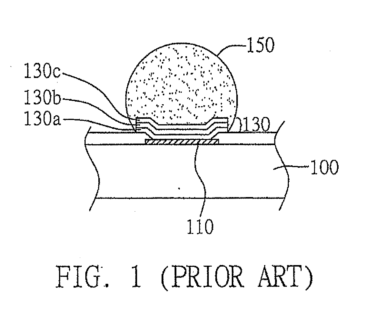
[0037]As shown in FIG. 5A, a semiconductor device 50 with a connection pad 500 formed thereon is provided and a passivation layer 51 exposing the connection pad 500 is formed on the semiconductor device 50 such that an under bump metallurgy (UBM) structure 52 is formed on the connection pad 500 of the semiconductor device, wherein the UBM structure 52 is sized larger than the connection pad 500. The semiconductor device 50 may be used in a substrate for semiconductor package or a tape carrier such as a tape carrier package (TCP). The semiconductor device 50 may also be used in a printed circuit board for assembling electrical components in second phase. Furthermore, the semiconductor device may be used in a wafer / chip integrated circuit structure that may subsequently be used as a fli...

second preferred embodiment

[0045]FIGS. 6A to 6F are schematic cross-sectional views showing a method of fabricating a conductive bump structure for a semiconductor device according to a second embodiment of the present invention.

[0046]As shown in FIGS. 6A and 6B, a semiconductor device 60 with a connection pad 600 formed thereon is provided and a passivation layer 61 exposing the connection pad 600 is formed on the semiconductor device 60. Thereafter a metal layer 620 and a resist layer 63 are applied in sequence over the semiconductor device 60, wherein the resist layer 63 has an opening 630 corresponding to the connection pad 600 for exposing a portion of the metal layer 620. The metal layer 620 may have one or more layers and be used as a current conduction path during plating process for forming solder, as well as reserving a portion of metal layer 620 at a position corresponding to the connection pad 600 for subsequently forming an UBM structure. The metal layer 620 may be formed by physical methods such...

third preferred embodiment

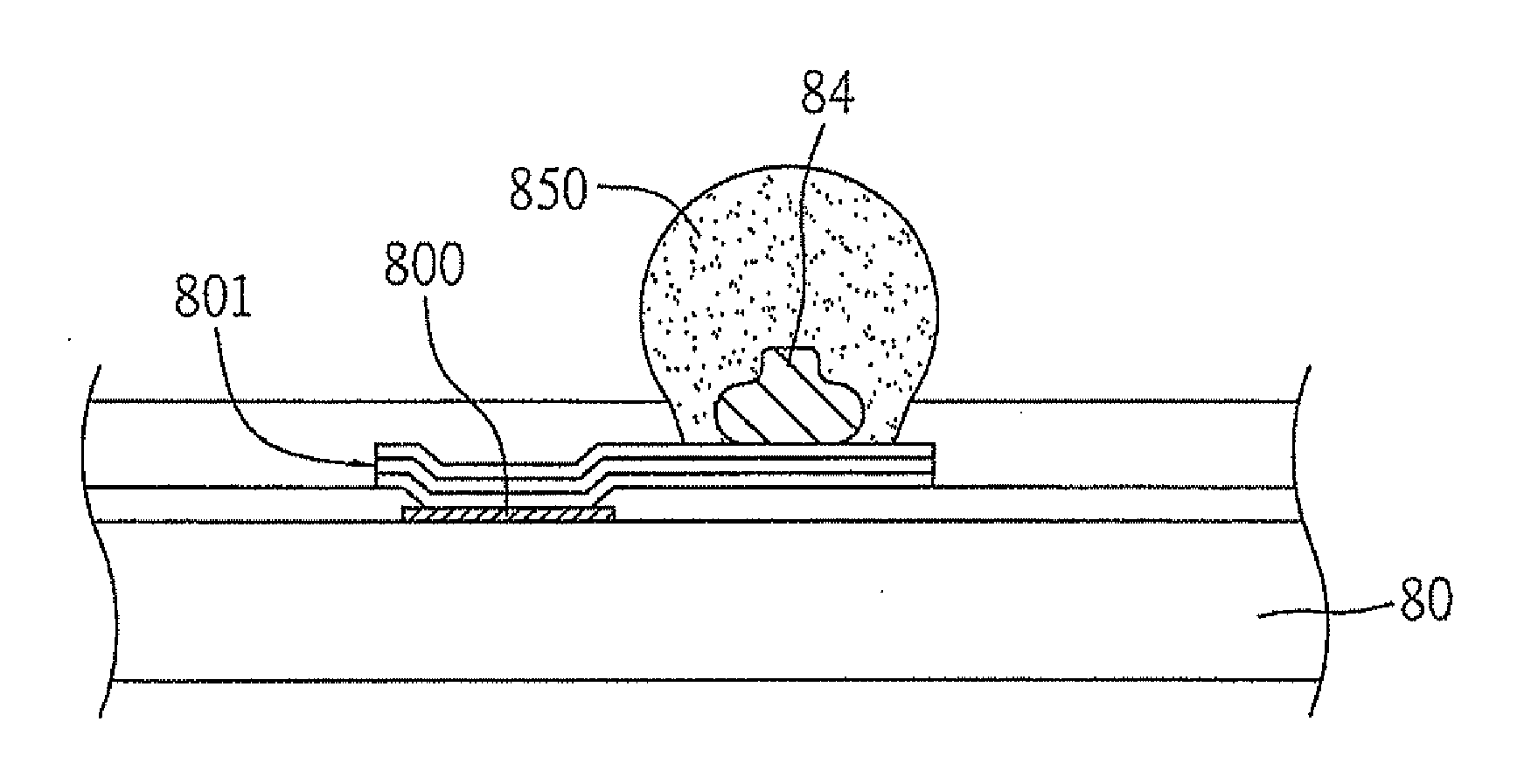
[0051]FIG. 7 is a schematic cross-sectional view showing a conductive bump structure for a semiconductor device according to a third embodiment of the present invention.

[0052]The method of fabricating the conductive bump structure for semiconductor device in the present embodiment is similar to the method disclosed in the first or the second embodiment; however the differences are that the present embodiment comprises a conductive bump structure that is applied to a wafer level chip scale package (WLCSP) structure, and a redistribution layer 701 (RDL) electrically connecting to and formed on at least a connection pad 700 of a chip 70, wherein the existing connection pad 700 may be redistributed through the redistribution layer 701 electrically connected to the connection pad 700. Subsequently, an UBM structure 72 and a metal bump 74 are formed on a suitable position on the redistribution layer 701 that serves as a new connection pad 702, wherein the metal bump 74 is sized smaller th...


PUM


Abstract

A conductive bump structure for a semiconductor device and a method for fabricating the same are provided. A metal bump is formed on an under bump metallurgy (UBM) structure electrically connected to and formed on a connection pad of the semiconductor device, wherein the metal bump is sized smaller than the UBM structure. Subsequently, a solder bump is mounted on the UBM structure and encapsulates the metal bump, so as to increase the bonding area and simultaneously allow the solder bump to be sufficiently wetted on the UBM structure to enhance bonding stress of the solder bump.

Description

FIELD OF THE INVENTION[0001]The present invention relates to conductive bump structures for semiconductor devices and methods for fabricating the same, and more particularly, to a solder bump structure formed on a semiconductor device and a method for fabricating the same.BACKGROUND OF THE INVENTION[0002]Along with evolution of semiconductor fabrication technology and boosting circuit functions of chips, demands for various portable products in the fields of communication, network and computer technology have increased dramatically. In order to meet ever-increasing demands for miniaturized electronic products, advanced semiconductor packaging techniques such as ball grid array (BGA), flip chip, chip size package (CSP) and wafer level chip scale package (WLCSP) are required and become more popular as such packaging techniques are capable of reducing size and area of integrated circuit while forming a high-density semiconductor package with multi-pins.[0003]For instance, one of the ma...

Claims


Application Information

Patent Timeline
Patent Type & Authority Applications(United States)
IPC IPC(8): H01L21/60
CPCH01L24/11H01L2224/1134H01L2924/014H01L2924/01033H01L2924/01023H01L2924/00013H01L24/13H01L2924/14H01L2924/01327H01L2924/01082H01L2924/01079H01L2224/1147H01L2224/131H01L2224/13144H01L2224/13147H01L2224/1357H01L2224/136H01L2924/01013H01L2924/01022H01L2924/01029H01L2924/01046H01L2924/01047H01L2924/01074H01L2924/01078H01L2924/00014H01L2224/13099H01L2224/05569H01L2224/05024H01L2224/05008H01L2224/05022H01L2224/0508H01L2224/05548H01L2224/05567H01L2224/05573H01L2224/05001H01L2224/05572H01L2224/05124H01L2224/05155H01L2224/05624H01L2224/05644H01L2224/05647H01L2224/05655H01L2224/05664H01L2224/05666H01L2224/05684H01L24/05H01L24/03H01L2224/023H01L2924/0001
Inventor KE, CHUN CHIHUANG, CHIEN-PINGJIUNG, DON-SONWANG, YU-PO
Owner SILICONWARE PRECISION IND CO LTD
Why Eureka
Try Eureka