
Metal oxynitride thin film transistors and circuits

a thin film transistor and metal oxynitride technology, applied in transistors, semiconductor devices, electrical apparatus, etc., can solve the problems of relatively low circuit densities, pixel aperture, and material not used in mass production, and achieve the effect of increasing the mobility of the charge carrier and switching speed

Active Publication Date: 2010-12-02
QIU CINDY X +3
View PDF3 Cites 33 Cited by
  • Summary
  • Abstract
  • Description
  • Claims
  • Application Information

AI Technical Summary

Benefits of technology

[0011]One object of this invention is to provide a new class of TFTs and circuits with metal oxynitrides as the active channel materials to increase the charge carrier mobility and switching speed.
[0012]One other object of this invention is to provide a new class of TFTs and circuits with metal oxynitrides as the active channel materials to reduce the joule heating during switching and to improve thermal stability.
[0014]Still another object of this invention is to provide a new class of TFTs and circuits with metal oxynitrides as the active channel materials to increase the frequency of operation.

Problems solved by technology

However, due to its large OFF state current and its poor thermal stability, the above materials were not used in mass productions for electronic products involving TFTs.
However, amorphous silicon has a relatively low charge carrier mobility (˜1 cm2 / V-s), therefore, it suffers from relatively low circuit densities (low pixel aperture) and slow switching speeds because substrates are processed at relatively low temperature (<350° C.).
Because of the high processing temperatures, expensive substrates are needed to produce polycrystalline silicon TFTs for AM-LCDs, thus preventing this technology from being used in low cost production.
Hence, even though TFTs made of these metal oxides are suitable for driving of LCDs and OLEDs displays, the resistance between the drain and the source electrodes in the ON state is still considered high and the unwanted joule heating in the active channel layer is sizeable.
Furthermore, the charge carrier mobility of the metal oxides are not sufficiently high to form into devices and circuits for generating and manipulating of electrical signals in a frequency range from few tens of megahertz (MHz) to several gigahertz (GHz)—in the microwave range.

Method used


Image

  • Metal oxynitride thin film transistors and circuits
  • Metal oxynitride thin film transistors and circuits
  • Metal oxynitride thin film transistors and circuits

Examples


Embodiment Construction

TFTs With Metal Oxynitride Active Channels

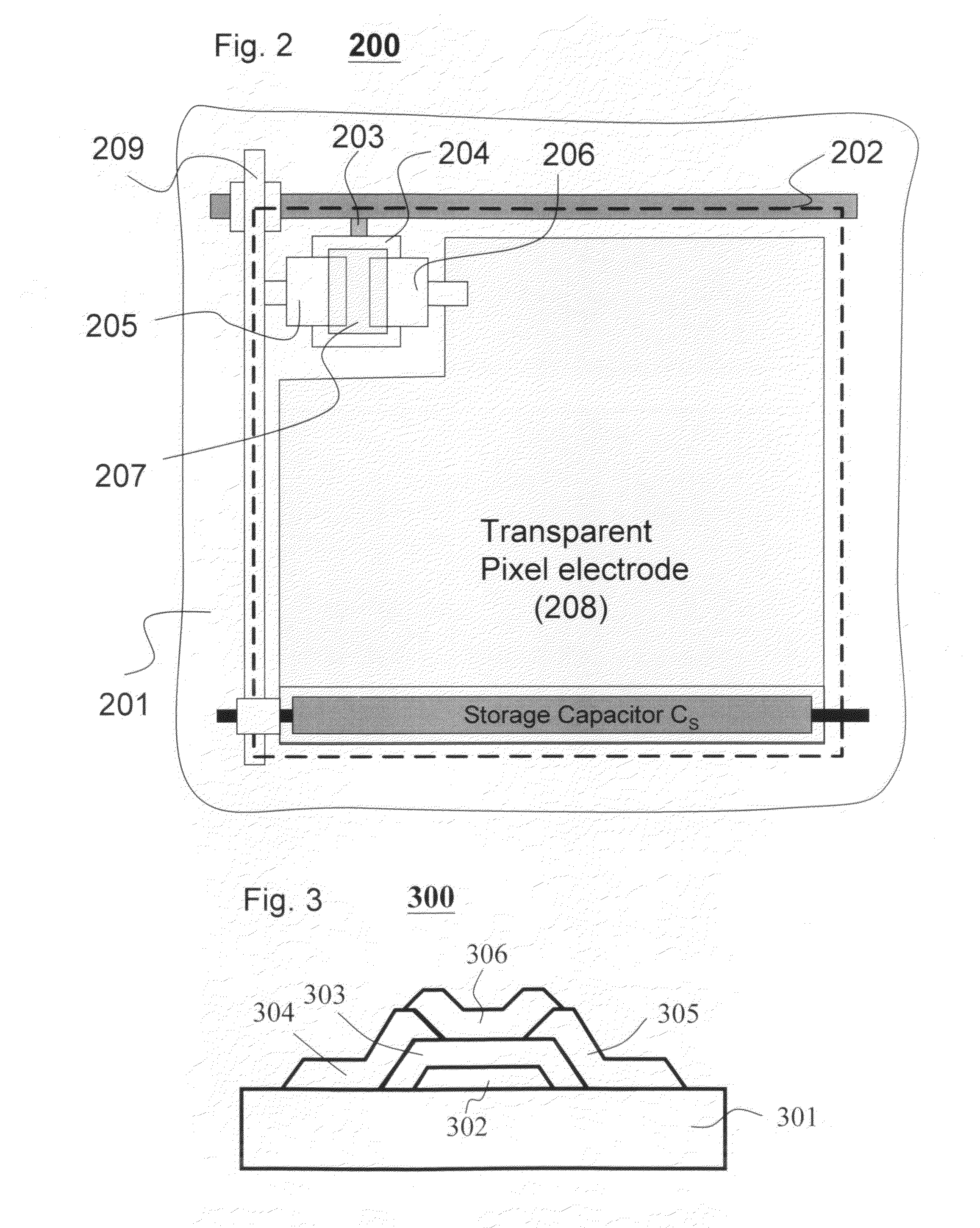
[0021]According to one embodiment of this invention, a thin film transistor (300) is provided (as illustrated in FIG. 3) to have a substrate (301), a first gate electrode (302), a first gate insulator (303), a drain (304), a source (305) and a first metal oxynitride active channel layer (306). In TFT (300), said first gate insulating layer (303) overlaps at least a portion of said first gate electrode (302); said source electrode (304) overlaps a first potion of said first gate insulating layer (303); said drain electrode (304) overlaps a second portion of said first gate insulating layer (303). Said first metal oxynitride active channel layer (306) overlaps a portion of said first gate insulating layer (303), at least a portion of said source electrode (304) and at least a portion of said drain electrode (305) so that a continuous conducting channel may be induced to connect said drain and source electrodes when a voltage is applied to said...


PUM


Abstract

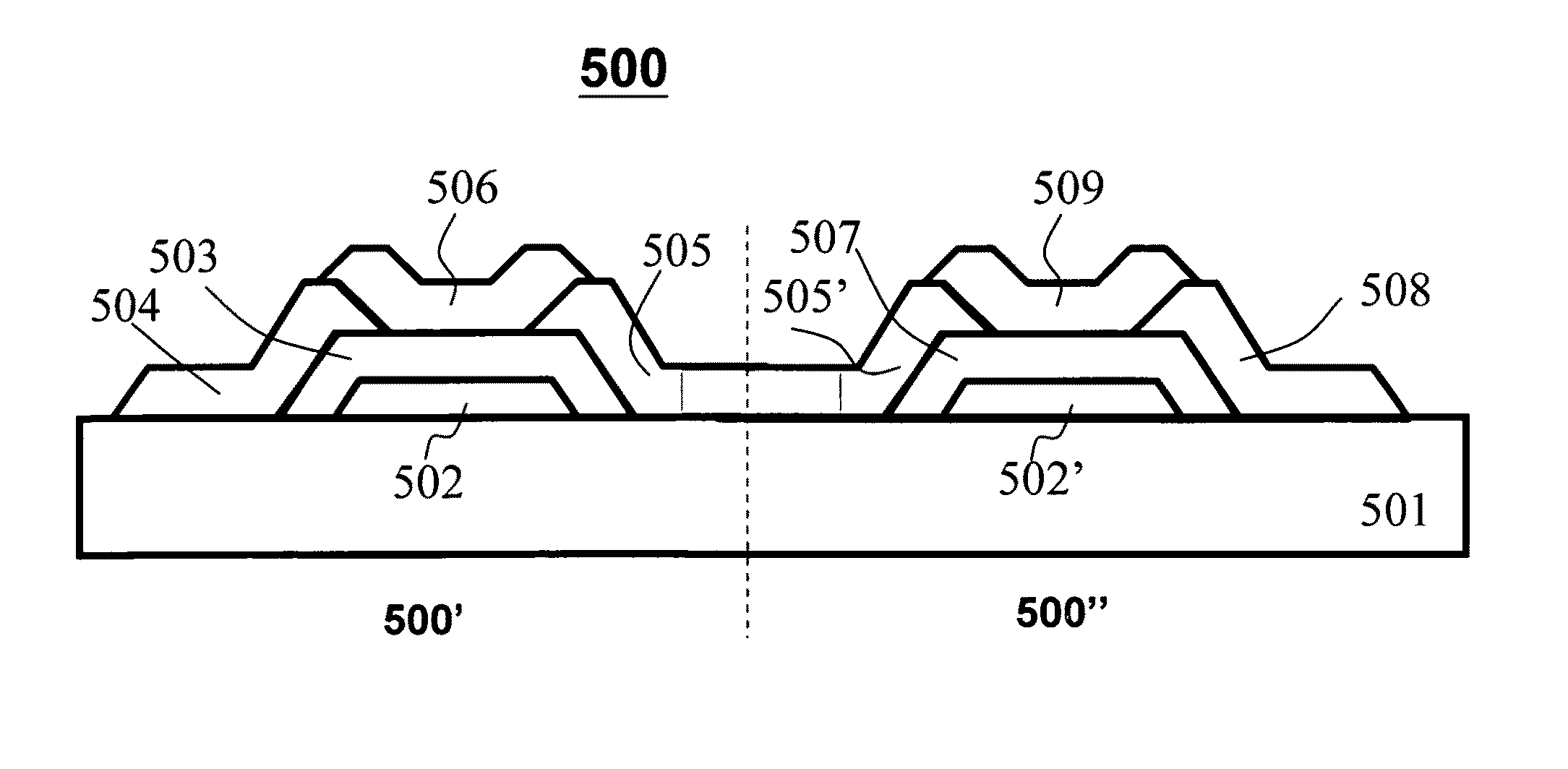
Thin film transistors and circuits having improved mobility and stability are disclosed in this invention to have metal oxynitrides as the active channel layers. In one embodiment, the charge carrier mobility in the thin film transistors is increased by using the metal oxynitrides as the active channel layers. In another embodiment, a thin film transistor having a p-type metal oxynitride active channel layer and a thin film transistor having an n-type metal oxynitride active channel layer are fabricated to forming a CMOS circuit. In yet another embodiment, thin film transistor circuits having metal oxynitrides as the active channel layers are provided.

Description

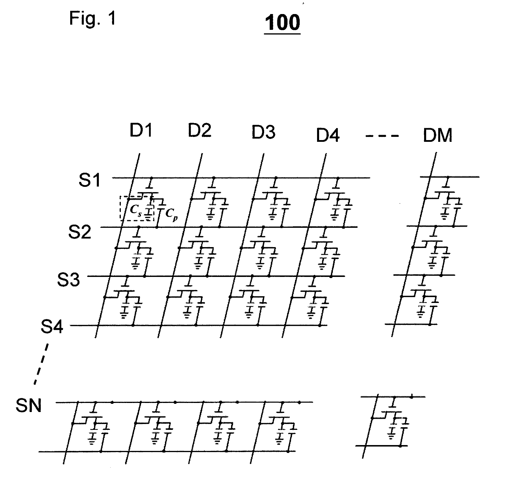
FIELD OF INVENTION [0001]This invention is related to thin film transistors for electronic and optoelectronic applications. More specifically, it relates to a family of thin film transistors with metal oxynitride channel and a family of thin film transistor circuits with metal oxynitride channel for flat panel electronic display, imaging and microwave applications.BACKGROUND OF THE INVENTION [0002]In large area electronic circuits including active-matrix liquid crystal display (AM-LCD) technology, active-matrix organic light emitting displays (AM-OLED) and x-ray imagers, thin film transistors are used to form the switching circuits. For example, in an AM-LCD display, an array of TFTs are used as the active “switches”, each TFT controls one of the pixels of the displays. As shown in FIG. 1, an LCD display (100) consists of a two dimensional array of pixels having data lines (D1-DM) and gate selection lines (S1-SN). A TFT is inserted between the gate selection line and the data line a...

Claims


Application Information

Patent Timeline
Patent Type & Authority Applications(United States)
IPC IPC(8): H01L29/786
CPCH01L29/7869
Inventor QIU, CINDY X.SHIH, YI-CHIQIU, CHUNONGSHIH, ISHIANG
Owner QIU CINDY X
Learn More