Touch Panel Manufacturing Method

a manufacturing method and touch panel technology, applied in the field of manufacturing methods, can solve the problems of deficiency of wrong detection or inaccurate touch detection, damage to the physical characteristics of the sensing layer b>11/b>, and easy detachment of the touch panel

Inactive Publication Date: 2010-12-02
ETURBOTOUCH TECH
View PDF4 Cites 9 Cited by
  • Summary
  • Abstract
  • Description
  • Claims
  • Application Information

AI Technical Summary

Benefits of technology

[0012]The present invention provides a touch panel manufacturing method with simplified manufacturing process.
[0013]The present invention further provides a touch panel manufacturing method which would not damage physical characteristics of touch panel.
[0016]In the above-mentioned touch panel manufacturing method, the sensing layer is covered by the protective layer ahead, and a large quantity of heat or chemical substances accompanying with the formation of the electrode layer would not influence physical characteristics of the sensing layer. Therefore, the sensing layer can retain better physical characteristics such as electrical conductivity or electrical resistance, etc. Furthermore, since the formation of the protective layer is prior to the formation of the electrode layer, a contact area between the electrode layer and air can be reduced, the surface oxidization phenomenon of the electrode layer can be avoided and thus the electrode layer can achieve better physical characteristics such as electrical conductivity or electrical resistance. Meanwhile, such an arrangement of the formation of the sensing layer prior to the formation of the electrode layer, compared with the arrangement of the formation of the electrode layer prior to the formation of the sensing layer in the prior art, the height difference of the protective layer at the periphery of the electrode layer can be effectively prevented and the occurrence of optical interference phenomena can be avoided.
[0017]In addition, in term of process simplification, since the processes for the formation of both the sensing layer and the protective layer are similar to each other, the sensing layer and the protective layer can be sequentially formed on the substrate in a same process. Meanwhile, the formation of the electrode layer with spaced electrodes can be completed only by one time firing process, so that increased production speed and production capacity with respect to the prior art can be achieved.
[0023]Regardless of which one of the above-mentioned touch panel manufacturing methods, all of them can achieve the following advantages that: the first sensing layer and the second sensing layer are avoided to be surface oxidized resulting from long-time exposure to air in post-process. Meanwhile, during the formation of the first electrode layer and the second electrode layer, the physical characteristics of the first sensing layer and the second sensing layer are not influenced. Furthermore, after the formation of the first protective layer and the second protective layer, no optical interference phenomena occur.

Problems solved by technology

In one aspect, during the formation of the metallic electrode layer 12 on the surface of the sensing layer 11, a large quantity of heat or chemical substances would accompany therewith, which would easily result in the physical characteristics of the sensing layer 11 being damaged, e.g., the changes of electrical conductivity, electrical resistance, etc.
Therefore, when the capacitive type touch panel is in use, the deficiency of wrong-detection or inaccurate touch detection would be easily occurred.
Accordingly, the electrode layer 13 would be easily damaged in use, and even the height difference would cause an optical interference issue.
In even still another aspect, when the capacitive type touch panel 1 is in manufacturing, manufacturing steps are too complicated.
However, processes for the above-mentioned steps are not the same and required manufacture machines also are not the same, which results in the entire manufacturing process being too complicated.

Method used


Image

  • Touch Panel Manufacturing Method
  • Touch Panel Manufacturing Method
  • Touch Panel Manufacturing Method

Examples


Embodiment Construction

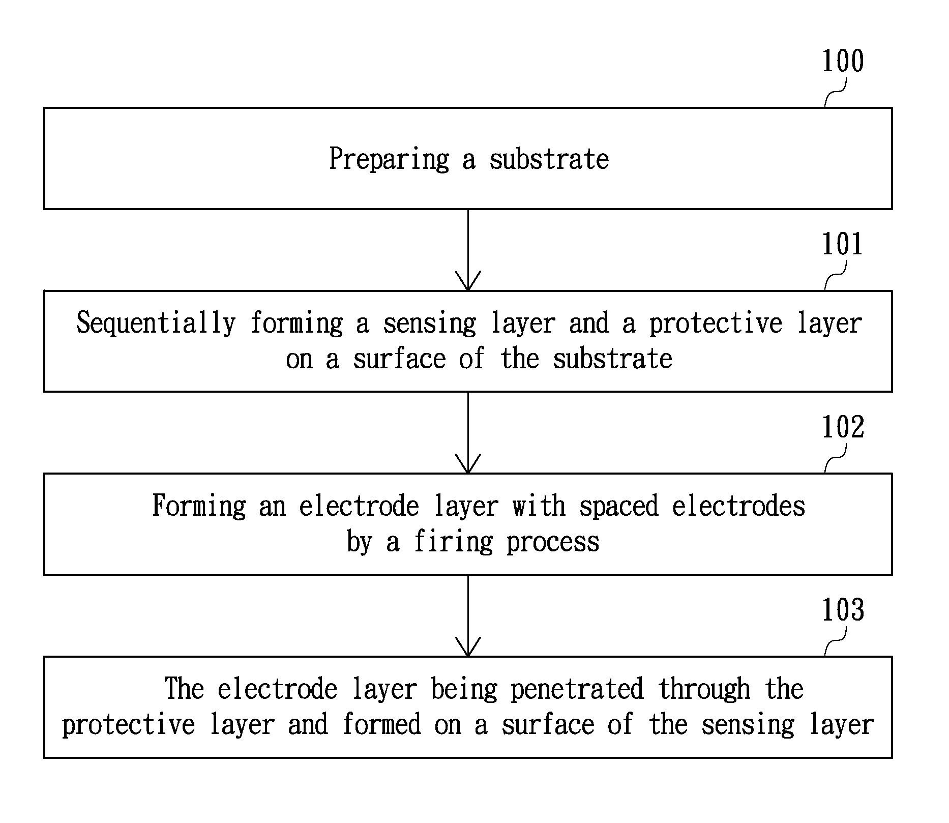
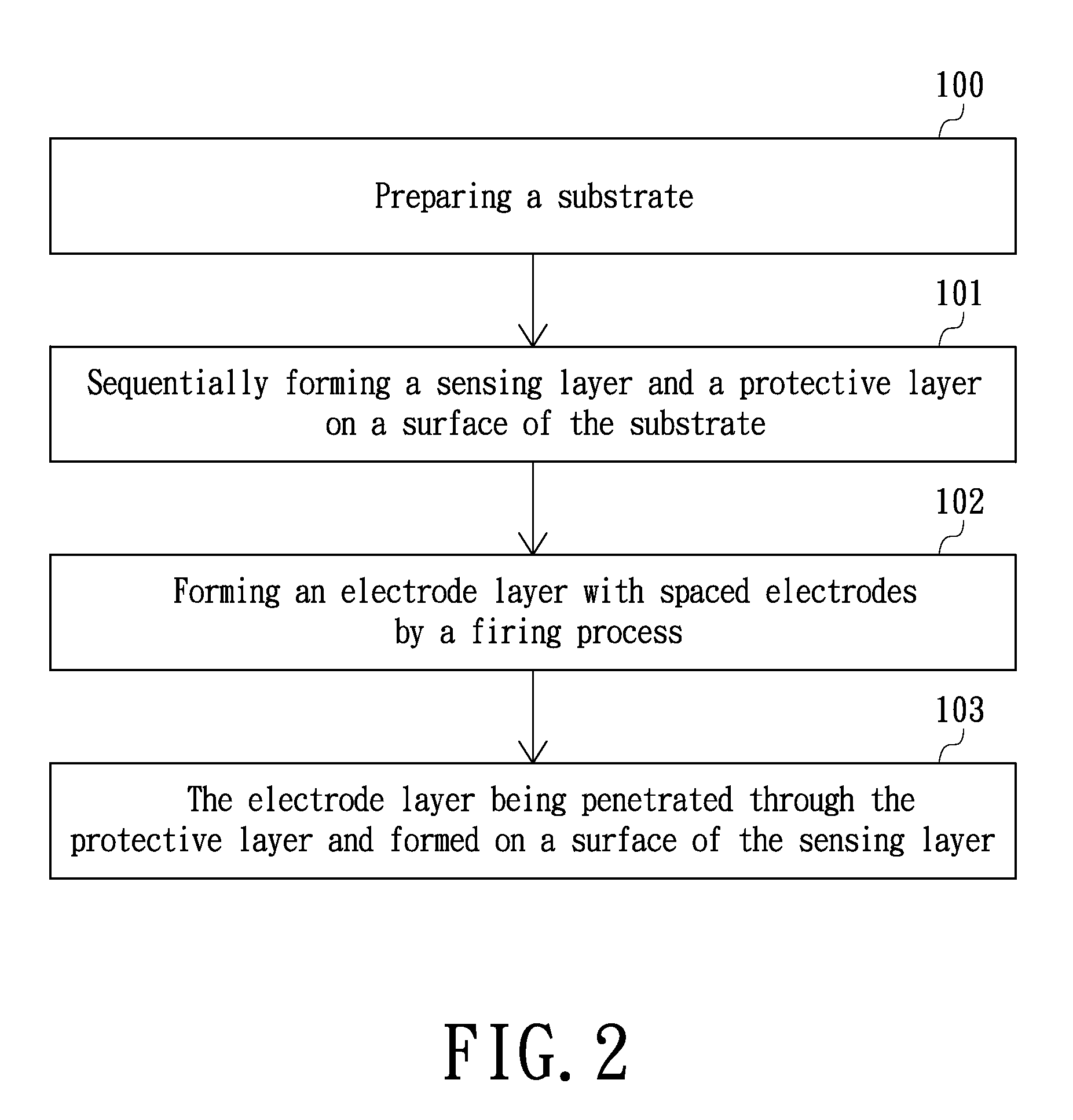
[0035]Referring to FIGS. 2 through 4, respectively illustrating a flow chart, a flow diagram (1) and a flow diagram (2) of a touch panel manufacturing method in accordance with a preferred embodiment of the present invention. The touch panel manufacturing method includes several steps as follows.

[0036]A substrate is prepared (Step 100). The substrate 20 may be made of glass and is for supporting the touch panel 2, so that the touch panel 2 has a particular hardness and facilitates in combination with an external electronic device.

[0037]A sensing layer and a protective layer are sequentially formed on a surface of the substrate 20 in that order (Step 101). The sensing layer 21 may be made of indium tin oxide (ITO). The protective layer 22 may be made of cyclo-olefin copolymer (COC), polyethylene terephthalate (PET), silicon dioxide (SiO2) or plastic, etc. The formation of the sensing layer 21 and the protective layer 22 on the surface of the substrate 20 can be performed by a method ...


PUM

PropertyMeasurementUnit
transmittanceaaaaaaaaaa
temperatureaaaaaaaaaa
transparentaaaaaaaaaa

Abstract

In a touch panel manufacturing method, a substrate is prepared, a sensing layer and a protective layer are sequentially formed on the substrate, an electrode layer with spaced electrodes is formed by firing, and the electrode layer is penetrated through the protective layer and formed on a surface of the sensing layer. Since the sensing layer is covered by the protective layer before forming the electrode layer, the sensing layer can be avoided to be influenced by accompanying heat, chemical substances and / or oxygen gas, its intrinsic physical characteristics are retained and its periphery would not be damaged. Moreover, since the formation of the protective layer is prior to the electrode layer, the height difference formed at the periphery of the electrode layer and the optical interference phenomena both are prevented. Finally, the manufacturing process is simplified and thus production speed and production capacity are increased.

Description

BACKGROUND[0001]1. Technical Field[0002]The present invention generally relates to manufacturing methods and, particularly to a touch panel manufacturing method with simplified manufacturing process.[0003]2. Description of the Related Art[0004]Nowadays, with the rapid development of high-tech electronic information industry, consumer electronic products have become necessities of people's daily lives. Many consumer electronic products are continuingly moving toward the lightweight, thin, short and small trends and especially for a touch-sensitive liquid crystal display panel combined with information display and information input technologies. The touch-sensitive liquid crystal display panel is endowed with a liquid crystal display function as well as a touch-sensitive input function, and thus the practicability of the various consumer electronic products can be greatly enhanced. The touch-sensitive liquid crystal display panel predominantly is that combining a touch panel onto a li...

Claims


Application Information

Patent Timeline
Patent Type & Authority Applications(United States)
IPC IPC(8): B05D5/12C23C14/34
CPCG06F3/044G06F3/0445
Inventor WANG, XUEI-MIN
Owner ETURBOTOUCH TECH
Why Eureka
Try Eureka