Bio lab-on-a-chip and method of fabricating and operating the same

a bio lab and chip technology, applied in the field of bio labs on chips, can solve the problems of requiring separate devices, large amounts of bio samples and expensive reagents mixed therewith, and high cost of generic reagents, so as to reduce analysis costs, reduce fabrication costs, and rapid and precise analysis

Inactive Publication Date: 2010-12-02
ELECTRONICS & TELECOMM RES INST
View PDF13 Cites 20 Cited by
  • Summary
  • Abstract
  • Description
  • Claims
  • Application Information

AI Technical Summary

Benefits of technology

[0047]As described in detail above, according to the present invention, it is possible to transfer, stop, react, and sense a microfluid in the form of a micro-sized drop solution on a single chip. Accordingly, a bio lab-on-a-chip may be provided to reduce analysis cost by minimizing the consumption of a bio sample and reagents. Further, since all the processes of a chemical analysis are performed on a single chip, a bio lab-on-a-chip may be provided for a rapid and exact analysis. In addition, a bio lab-on-a-chip may be provided to reduce fabrication cost by replacing an expensive bulk substrate with a piezoelectric thin film. Additionally, a signal-processing unit can be integrated on a single chip using a general semiconductor manufacturing process. Therefore, this can be also applicable to various bio lab-on-a-chip fields such as a protein lab-on-a-chip, polymerase chain reaction (PCR), DNA lab-on-a-chip and a micro biological / chemical reactor.

Problems solved by technology

Since most of the generic reagents are generally expensive, a reproducible and contamination-free chemical analysis must be performed using a minimum volume of a bio sample.
Since this type of the microfluidic control system has a continuous flow of a fluid consisting of a bio sample, the system has the disadvantage that the larger amounts of the bio sample and the expensive reagents mixed therewith should be consumed to sense a bio marker substantially.
The system also has the disadvantage that a separate device should be required to maintain the dispersion of a target bio material such as protein, cell, and DNA, in the fluid.
The quartz bulk substrates in the bio sensor are disadvantageous in that they are expensive and hardly applied to a general semiconductor manufacturing process based on typical silicon substrates.
In addition, when a microfluidic control system and a detection sensor are fabricated on a single chip, peripheral signal processing circuits, for example, amplifier circuit, analog / digital converter, cannot be integrally formed.

Method used


Image

  • Bio lab-on-a-chip and method of fabricating and operating the same
  • Bio lab-on-a-chip and method of fabricating and operating the same
  • Bio lab-on-a-chip and method of fabricating and operating the same

Examples


Embodiment Construction

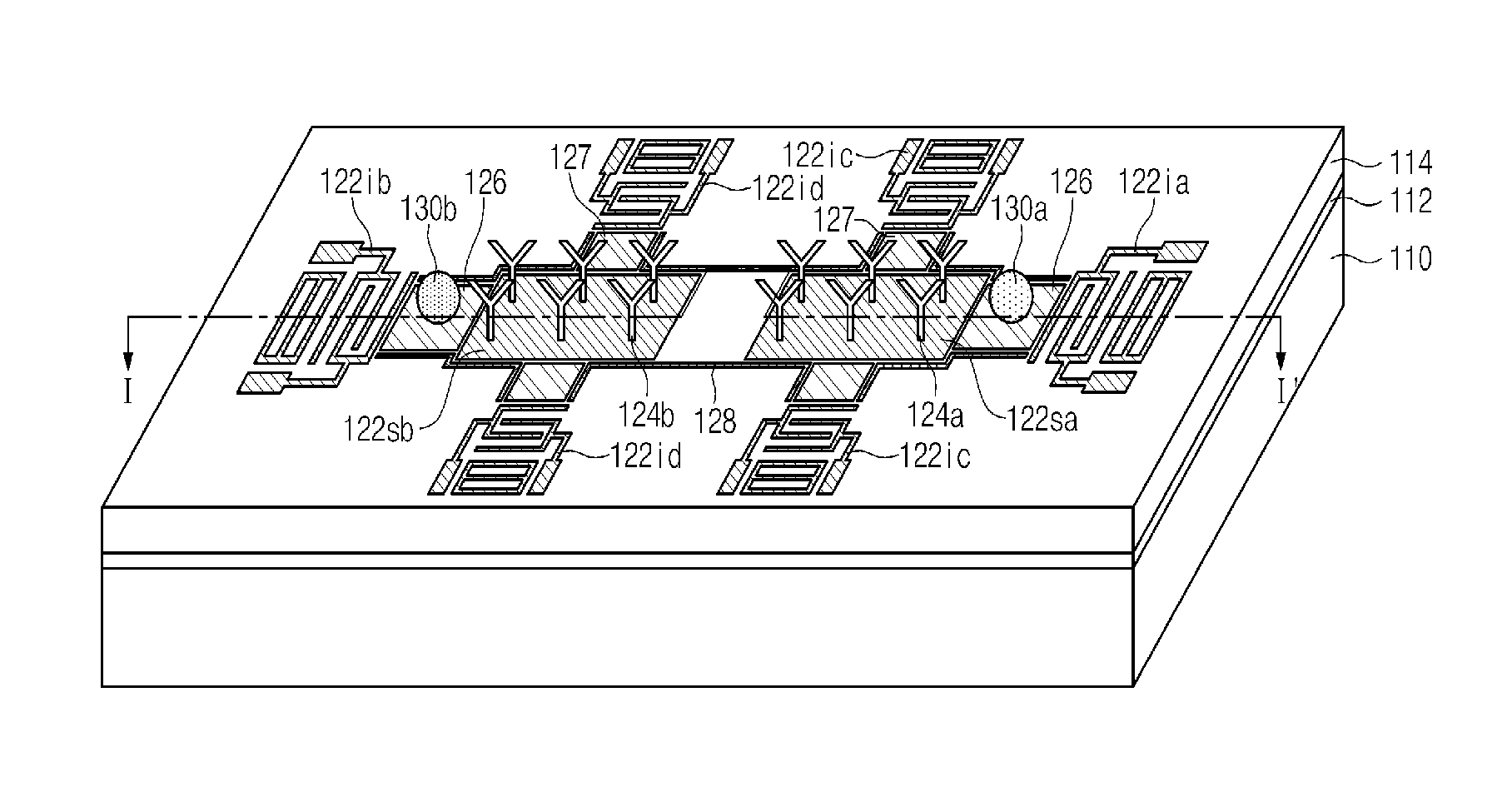
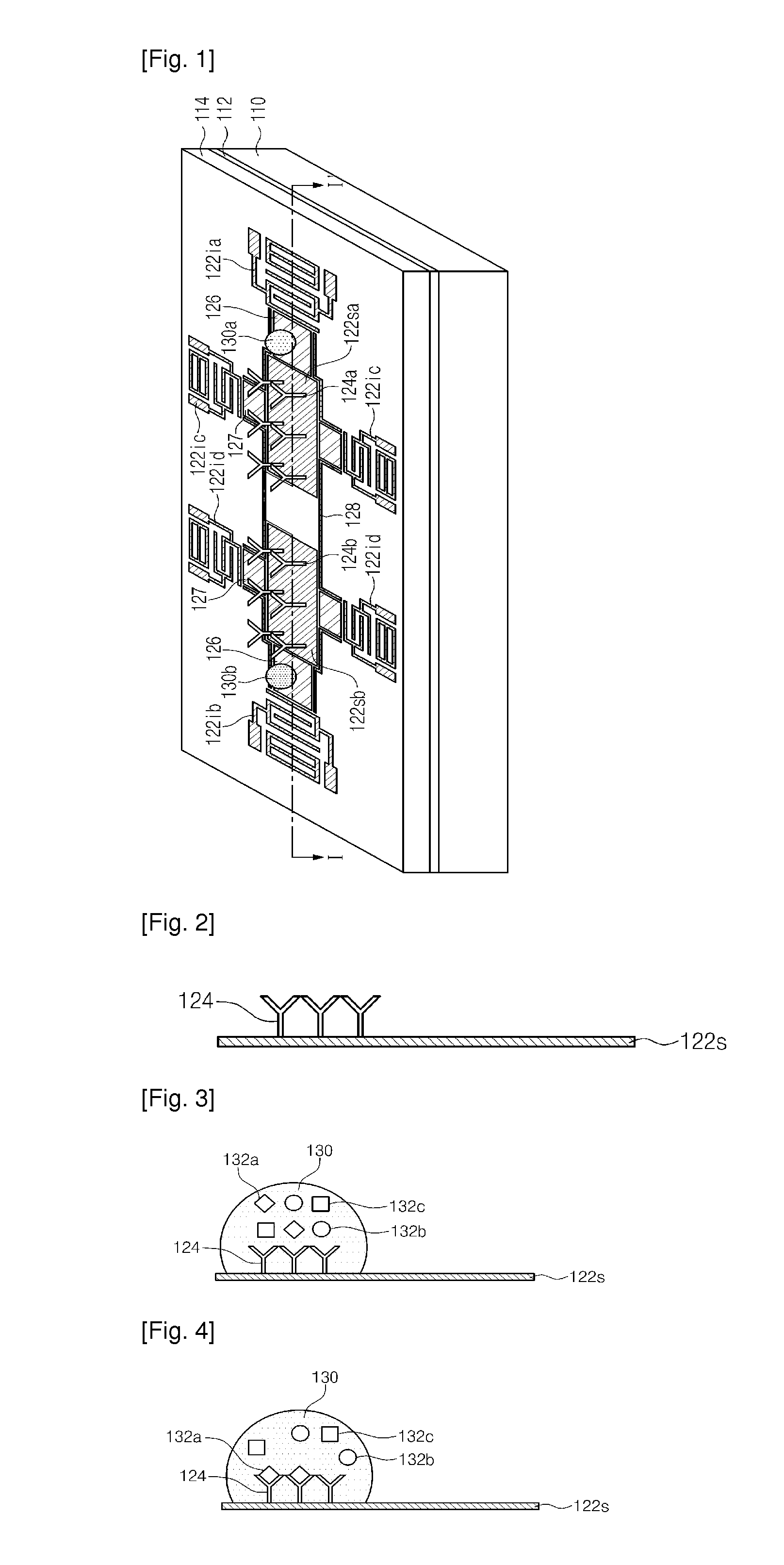
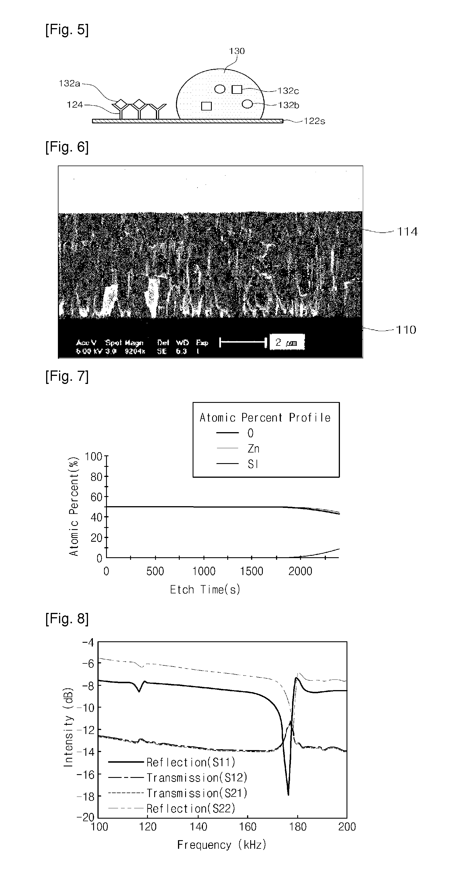
[0059]Preferred embodiments of the present invention will be described below in more detail with reference to the accompanying drawings. The present invention may, however, be embodied in different forms and should not be construed as limited to the embodiments set forth herein. Rather, these embodiments are provided so that this disclosure will be thorough and complete, and will fully convey the scope of the present invention to those skilled in the art. Additionally, because the reference numerals have been used to clarify a preferred embodiment, their sequences in description may not necessarily be limited to a numerical order. In the figures, the dimensions of layers and regions are exaggerated for clarity of illustration. It will also be understood that when a layer (or film) is referred to as being ‘on’ another layer or substrate, it can be directly on the other layer or substrate, or intervening layers may also be present. Further, it will be understood that when a layer is r...


PUM

PropertyMeasurementUnit
thicknessaaaaaaaaaa
thicknessaaaaaaaaaa
thicknessaaaaaaaaaa

Abstract

Disclosed is a bio lab-on-a-chip. The bio lab-on-a-chip is provided on a piezoelectric thin film on a substrate, and includes a sensing unit to sense a bio signal and a fluidic control unit which controls a transfer of a microfluid adjacent to the sensing unit. Provided is also a method of fabricating the bio lab-on-a-chip. The method includes the steps of forming a piezoelectric thin film, forming a sensing unit to sense a bio signal of a microfluid on the piezoelectric thin film, and forming a fluidic control unit located adjacent to the sensing unit.

Description

TECHNICAL FIELD[0001]Hi The present invention relates to a bio-micro electro mechanical system and a method of fabricating the same, and more particularly to a bio lab-on-a-chip and methods of fabricating and operating the same.[0002]The present invention has been derived from research undertaken as a part of IT R & D program of the Ministry of Information and Communication and Institution of Information Technology Association (MIC / IITA) [2006-S-007-02], Ubiquitous health monitoring module and system development.BACKGROUND ART[0003]Generally, in the field of bio-micro electro mechanical systems (Bio-MEMS), to perform processes such as early diagnosis of diseases and / or chemical analysis on a small chip, a microfluidic control capable of transferring, stopping, mixing, and reacting an ultra-low volume fluid, and an integration of sensors capable of sensing bio markers, for example, protein, deoxyribonucleic acid (DNA), related to diseases must be required.[0004]In the Bio-MEMS field,...

Claims


Application Information

Patent Timeline
Patent Type & Authority Applications(United States)
IPC IPC(8): G01N33/543G01N30/96
CPCB01L3/502707B01L3/50273B01L2200/0673B01L2300/0636B01L2300/0645B01L2300/0816B01L2300/089B01L2300/161B01L2400/0436B01L2400/0496G01N33/54366G01N33/5438
Inventor LEE, DAE SIKPARK, RAE MANMAENG, SUNG LYULJUNG, MOON YOUNPARK, SEON HEEYOON, HYUN CHUL
Owner ELECTRONICS & TELECOMM RES INST
Why Eureka
Try Eureka