Method for Manufacturing Hetero-Bonded Wafer

a technology of hetero-bonded wafers and manufacturing methods, applied in the direction of electrical equipment, semiconductor devices, semiconductor/solid-state device details, etc., can solve the problems of debonding, bow/warp cracking, debonding, etc., to solve high cost, and increase the first bonding strength. , the effect of solving the thermal stress problems of hetero-bonded wafers

Inactive Publication Date: 2010-12-09
KIM YOUNG HAE
View PDF7 Cites 54 Cited by
  • Summary
  • Abstract
  • Description
  • Claims
  • Application Information

AI Technical Summary

Benefits of technology

[0012]To solve the thermal stress issues in heterogeneous wafer bonding and the high cost of conventional die-to-wafer bonding method, an embodiment of a method for manufacturing a hetero-bonded wafer comprises: i) bonding two dissimilar wafers at low temperature or more preferably at room temperature to avoid thermal stress, ii) fragmenting one of the bonded wafer pair into a plurality of small segments, iii) rebonding the bonded wafer pair at an elevated temperature to increase the first bonding strength or form a new strong bond between the two bonding wafers.

Problems solved by technology

These conventional wafer bonding techniques require high bonding temperatures ranging from 200° C. to 400° C. Bonding of dissimilar materials having different thermal expansion coefficients (TEC) at such a high temperature gives rise to thermal stresses and strains that lead to defect generation, debonding, bow / warp and cracking.
But, non-silicon based devices made of compound semiconductors and piezoelectric materials have not been successful using silicon cap wafer bonding due to TEC mismatch problems.
For instance, Lithium niobate (LiNbO3) and Lithium tantalite (LiTaO3), commonly used for surface acoustic wave (SAW) filter fabrication, have several times larger TEC than silicon or LTCC, thus wafer bonding of silicon and piezoelectric materials has significant thermal stress problems.
However, serious thermal stress imposed by subsequent heat treatment limits the allowed temperature range and obtainable bond strength.
However, one drawback of the SAB is high cost of manufacturing due to the high vacuum level of about 1×10⁻⁶ Torr or above.
Although room temperature direct bonding techniques are potentially promising to solve the thermal stress issues for heterogeneous wafer bonding, it has several intrinsic obstacles hard to be overcome.
For example, surface cleanness and smoothness are very critical for successful direct bonding, but practically such conditions are hardly to be met in the case of processed wafers having a variety of devices and surface conditions.
Therefore, contact pads or solder bumps are required but can produce a significant surface topology problem.
However, conventional die-to-wafer bonding method needs complicated manufacturing steps, such as singulating dies from a donor wafer, cleaning dies, and bonding each of the dies onto a receiving wafer, and therefore it is not cost effective.

Method used


Image

  • Method for Manufacturing Hetero-Bonded Wafer
  • Method for Manufacturing Hetero-Bonded Wafer
  • Method for Manufacturing Hetero-Bonded Wafer

Examples


Embodiment Construction

[0030]Before describing embodiments in detail, it is to be understood that the invention is not limited to specific materials, methods of wafer bonding, and application area of hetero-bonded wafers. The embodiments will be described more in detail hereinafter with reference to the accompanying drawings, in which preferred embodiments of the invention are shown. Furthermore, like reference numerals designate corresponding parts throughout the several views.

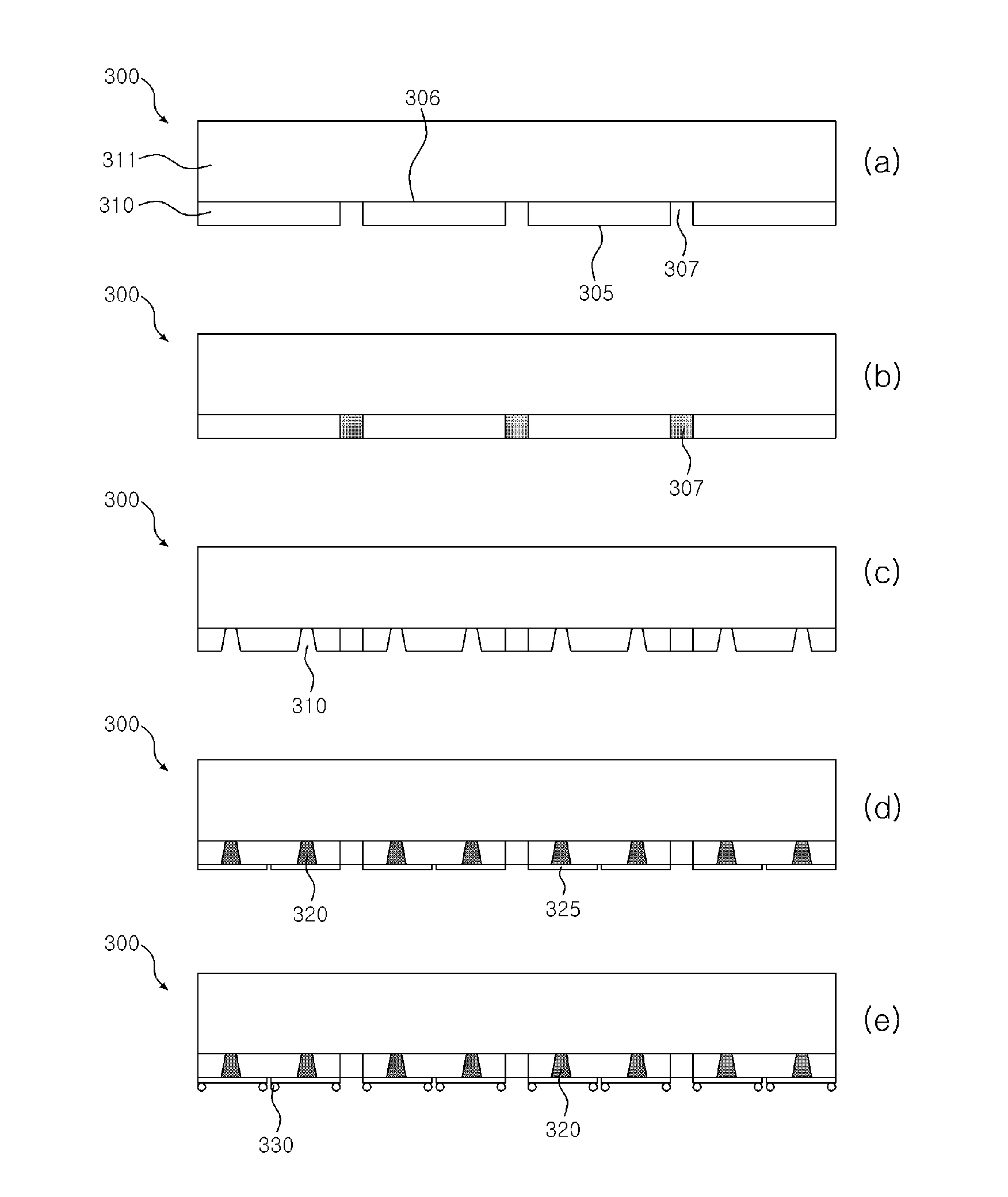
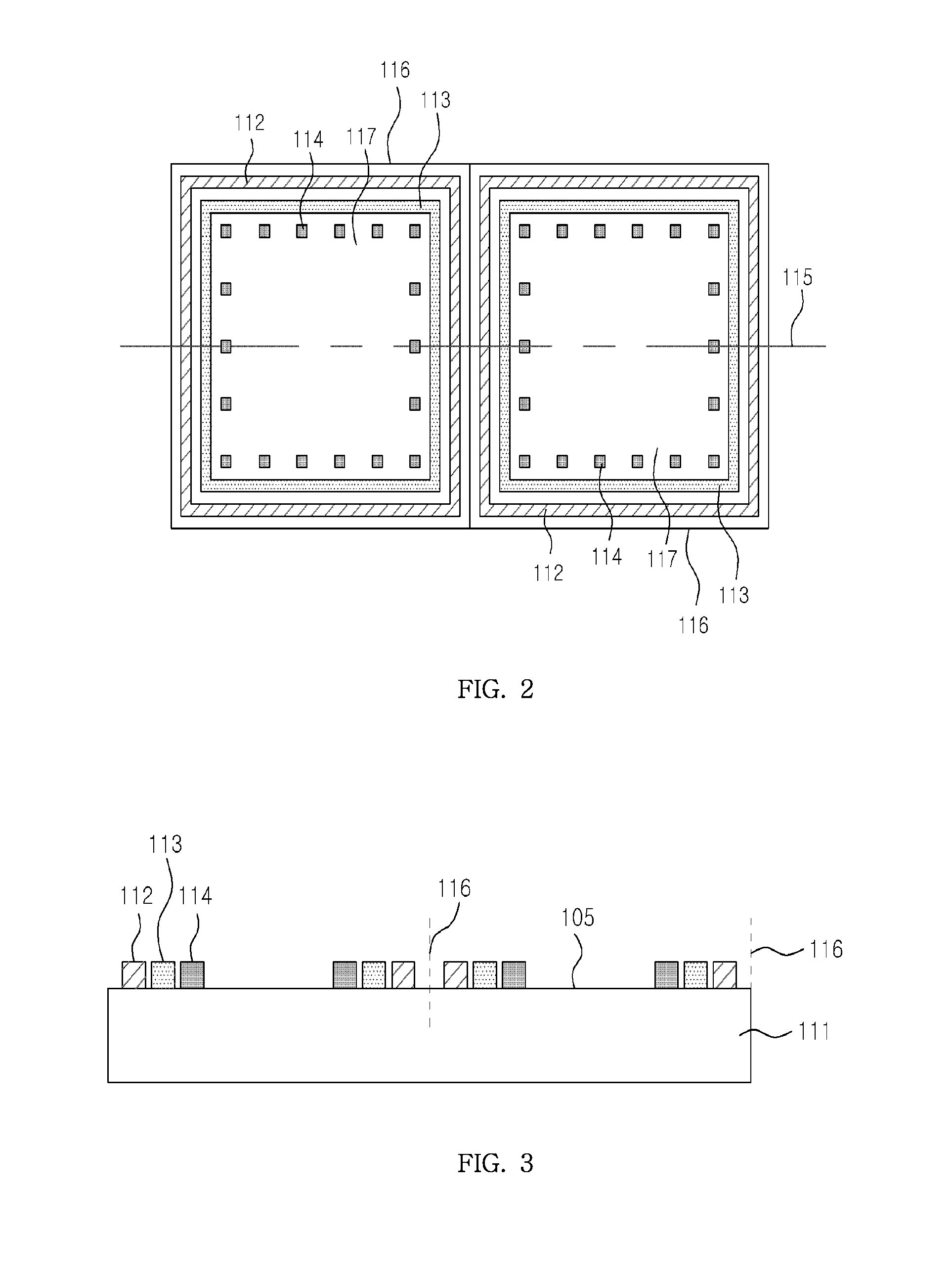
[0031]FIG. 1 is a flow diagram illustrating a method 50 for manufacturing a hetero-bonded wafer according to an exemplary embodiment. The method comprises: i) step S100 preparation of a first wafer and step S200 preparation of a second wafer to be bonded with each other; ii) step S110 formation of bonding means and electrical interconnection means on the bonding surface of the first wafer, and step S210 formation of bonding means and electrical interconnection means on the bonding surface of the second wafer; iii) step S120 formati...


PUM


Abstract

A method for manufacturing a hetero-bonded wafer having a large mismatch of thermal expansion coefficient comprises forming a wafer bonding means and an electrical interconnection means on at least one bonding surface of two wafers to be bonded with each other, forming grooves in the bonding surface of one wafer along dicing lines with an interval between the grooves being equal to or an even multiple of a die width, bonding the two wafers at a temperature less than 200° C. thinning a back side of the grooved wafer such that at least a portion of the grooves is exposed, and rebonding the bonded wafer pair at an elevated temperature higher than the first bonding temperature. The method for manufacturing a hetero-bonded wafer can avoid wafer level bow/warp and also reduce debonding and cracking in individual segments induced by thermal stress due to a mismatch of thermal expansion coefficient. Embodiments of the method are useful for wafer level packaging and the fabrication of hybrid devices by heterogeneous wafer bonding.

Description

CROSS-REFERENCE TO RELATED APPLICATIONS[0001]This application claims the priority of Korean Patent Application No. 10-2009-0050859, filed Jun. 9, 2009 in the Korean Patent Office, which is incorporated herein by reference in its entirety.BACKGROUND[0002]1. Field of the Invention[0003]Embodiments generally relate to wafer bonding techniques, and more specifically to a method for manufacturing hetero-bonded wafers for the application of heterogeneous device integration and wafer level packaging.[0004]2. Description of the Related Art[0005]Heterogeneous device integration through the combination of dissimilar materials such as silicon, compound semiconductors, piezoelectric materials, etc., offers the potential to provide versatile functions not available from pure devices alone. One method for heterogeneous device integration has been wafer bonding technology. Wafer bonding techniques readily available today include anodic bonding, thermo-compression boding, eutectic bonding, diffusio...

Claims


Application Information

Patent Timeline
Patent Type & Authority Applications(United States)
IPC IPC(8): H01L23/48H01L21/50H01L21/302
CPCH01L21/187H01L21/76898H01L2924/1461H01L2924/13064H01L2224/29101H01L2924/0665H01L2924/014H01L2924/01074H01L2924/01033H01L2924/01023H01L2924/01006H01L2924/01005H01L2224/2919H01L2924/14H01L2924/10329H01L2924/09701H01L2924/01322H01L2924/01082H01L2924/01079H01L24/13H01L24/14H01L24/29H01L24/30H01L24/73H01L24/81H01L24/91H01L24/92H01L24/94H01L25/0657H01L25/50H01L2224/16H01L2224/32014H01L2224/73H01L2224/81193H01L2224/81801H01L2224/81894H01L2224/83194H01L2224/83894H01L2224/94H01L2224/95H01L2225/06513H01L2924/01013H01L2924/01029H01L2924/01047H01L2924/0105H01L2924/01078H01L2224/81H01L2224/11H01L2924/00H01L2924/3512H01L2924/351H01L2224/05573H01L2224/05568H01L2224/05611H01L2224/05624H01L2224/05644H01L2224/05647H01L2924/00014H01L2224/0554H01L2924/013H01L2224/05599H01L2224/0555H01L2224/0556H01L21/20
Inventor KIM, YOUNG HAELEE, SANG HWAN
Owner KIM YOUNG HAE
Why Eureka
Try Eureka