Gallium nitride for liquid crystal electrodes

a liquid crystal electrode and gallium nitride technology, applied in the direction of semiconductor devices, instruments, electrical apparatus, etc., can solve the problems of increasing the optical absorption of a steered optical beam, inherently lossy conductive thin film semiconductors, and using substrates that exhibit birefringence, so as to achieve less free carrier absorption and high electron mobility

Active Publication Date: 2010-12-23
RAYTHEON CO
View PDF16 Cites 16 Cited by
  • Summary
  • Abstract
  • Description
  • Claims
  • Application Information

AI Technical Summary

Benefits of technology

[0005]To overcome the above-noted drawback of using highly doped indium oxide conductors, and in accordance with the concepts, structures and techniques described herein, highly conductive gallium nitride high electron mobility transistor structures (GaN HEMTs) are deposited or otherwise disposed on a substrate material, the structure having a mobility that is higher than the mobility of indium oxide. Consequently, fewer carriers are needed to achieve the same conductivity achieved using the prior art indium oxide approach. This results in less free carrier absorption. Thus, the use of GaN HEMTs and spinel overcome the above-noted drawbacks with respect to optical absorption of a steered optical beam and birefringence which alters polarization of a steered optical beam.
[0006]To provide a relatively inexpensive structure while overcoming the above-noted drawback of using substrates (e.g. sapphire substrates) that exhibit birefringence or using expensive substrates (e.g. cubic spinel) which do not exhibit birefringence, in one embodiment, a GaN HEMT is deposited on large area, relatively inexpensive, single crystal silicon substrates. The GaN HEMT is then transferred to a substrate which is substantially optically transparent at wavelengths of interest and having little or no birefringence and having a cost which is less than the cost of single crystal spinel. Exemplary symmetric crystals suitable for such use include, but are not limited to fused silica, poly spinel and zinc sulfide (ZnS).
[0007]With this particular arrangement, a GaN HEMT having improved mobility is provided. The use of an aluminum nitride (AlN) interlayer results in the HEMT having increased conductivity from improved mobility since alloy scattering at the AlGaN / GaN interface is reduced by the insertion of the AlN interlayer. Furthermore, the deposition of the GaN HEMT on larger area relatively inexpensive silicon single crystal substrates with a subsequent transfer to an optically suitable substrate (e.g. a substrate which may be inexpensive and / or a non-birefringent material) separates out the material growth, which requires high quality single crystal substrates of compatible crystal structure, from the final mounting substrate which no longer needs to be even single crystal. Also, the use of large area wafers enables many more OPA elements to be fabricated and thus fewer wafers are needed than in prior art approaches.

Problems solved by technology

Such conductive thin film semiconductors are inherently lossy particularly in the infrared wavelengths due to their high electron concentrations and low carrier mobilities.
Thus, one drawback to using highly doped indium oxide as electrodes (e.g. in OPA elements) is that such electrodes increase optical absorption of a steered optical beam.
Another drawback with the above-described approach is the use of substrates that exhibit birefringence (e.g. sapphire substrates).
One drawback of crystal cubic spinel, however, is that it is relatively expensive compared with other substrate materials (e.g. compared with the cost of sapphire, for example).
Furthermore crystal cubic spinel substrates are only available in relatively small diameters (e.g. two-inch diameters).

Method used


Image

  • Gallium nitride for liquid crystal electrodes
  • Gallium nitride for liquid crystal electrodes
  • Gallium nitride for liquid crystal electrodes

Examples


Embodiment Construction

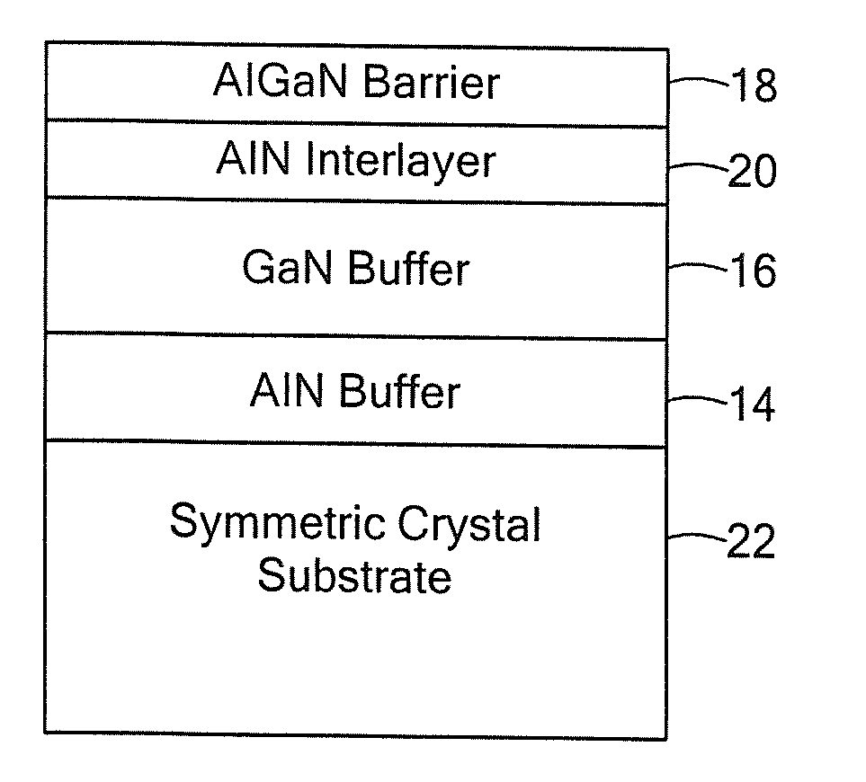
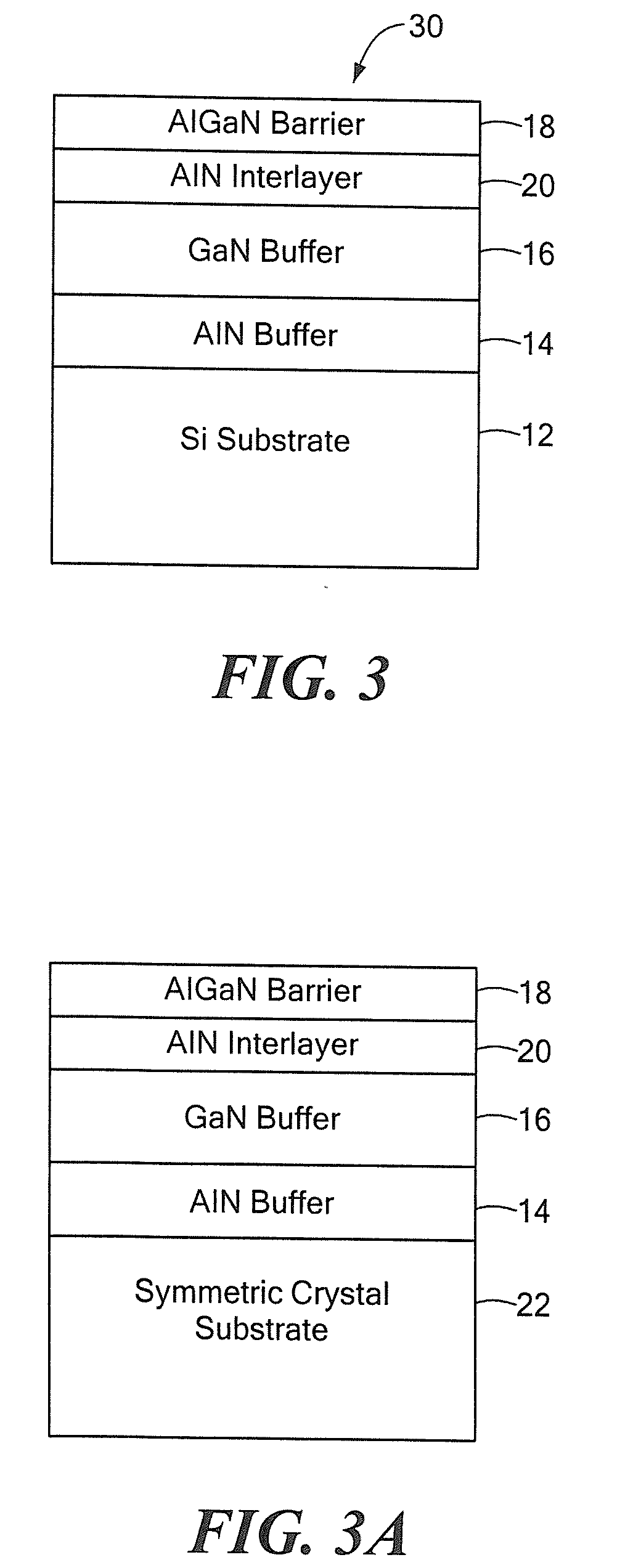
[0026]Referring now to FIG. 1 a transparent multi-electrode window using a gallium nitride (GaN) high electron mobility transistor (HEMT) structure includes a substrate 12 having an aluminum nitride (AlN) layer 14 disposed thereover with a semi-insulating gallium nitride (GaN) layer 16 disposed thereover. Substrate 12 may be provided from a number of materials, including but not limited to sapphire, SiC, Si, or Spinel. In one exemplary embodiment, GaN layer 16 is provided having a thickness typically in the range of about 1-3 microns (μm) and AlN layer 14 is provided having a thickness typically less than about 0.1 μm. In some applications, a thickness of 0.05 μm is preferred.

[0027]Disposed over the semi-insulating GaN layer 16 is a topmost AlN or AlxGa1-xN layer 18. In one embodiment, the topmost AlxGa1-xN layer 18 is provided having a thickness typically in the range of about 50-400 angstroms (Å) with about 200 Å being preferred in some applications.

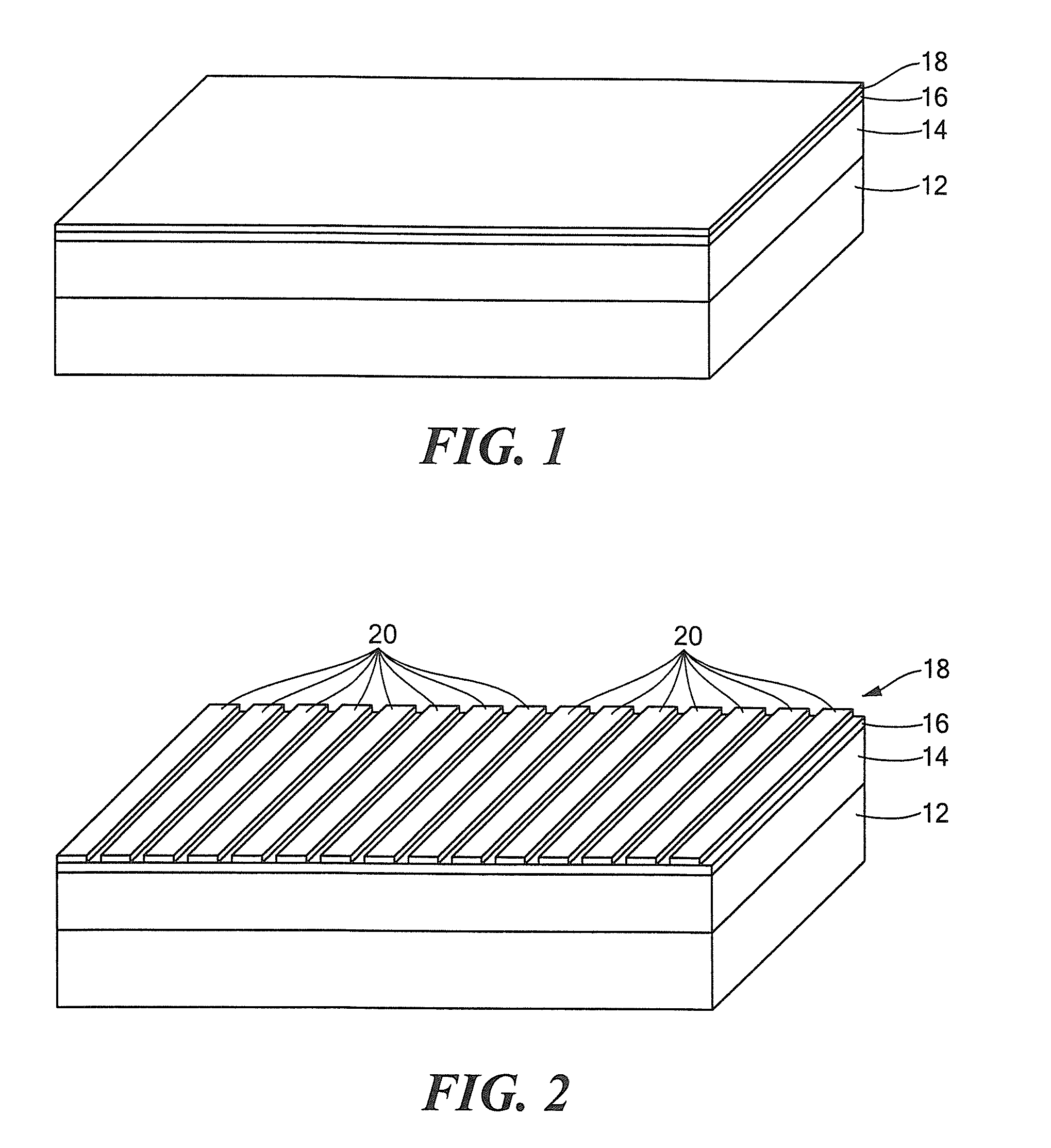
[0028]Referring now to FIG. 2, ...


PUM

PropertyMeasurementUnit
thicknessaaaaaaaaaa
thicknessaaaaaaaaaa
thicknessaaaaaaaaaa

Abstract

Described herein is a liquid crystal (LC) device having Gallium Nitride HEMT electrodes. The Gallium Nitride HEMT electrodes can be grown on a variety of substrates, including but not limited to sapphire, silicon carbide, silicon, fused silica (using a calcium fluoride buffer layer), and spinel. Also described is a structure provided from GaN HEMT grown on large area silicon substrates and transferred to another substrate with appropriate properties for OPA devices. Such substrates include, but are not limited to sapphire, silicon carbide, silicon, fused silica (using a calcium fluoride buffer layer), and spinel. The GaN HEMT structure includes an AlN interlayer for improving the mobility of the structure.

Description

FIELD OF THE INVENTION[0001]The structures and techniques described herein relate to liquid crystal devices and, more particularly to electrodes used in liquid crystal devices.BACKGROUND OF THE INVENTION[0002]As is also known in the art, liquid crystal (LC) devices utilize transparent electrodes which are necessary to establish electrical fields within the device to produce desired and controllable modifications to the liquid crystal optical material properties. One widely used method of electrode formation to date is the deposition of a thin-film semiconductor such as indium-tin-oxide (ITO) or In2O3. Such conductive thin film semiconductors are inherently lossy particularly in the infrared wavelengths due to their high electron concentrations and low carrier mobilities.[0003]Transparent conductors are required in various applications. For example, in optical phased arrays (OPA's) a steered beam passes through electrical conductors that bias and address the liquid crystal molecules ...

Claims


Application Information

Patent Timeline
Patent Type & Authority Applications(United States)
IPC IPC(8): H01L29/20H01L21/335
CPCG02F1/13439H01L29/7787H01L29/2003
Inventor RESLER, DANIEL P.HOKE, WILLIAM E.
Owner RAYTHEON CO
Why Eureka
Try Eureka