

Semiconductor device
a semiconductor and device technology, applied in the direction of pulse generators, pulse generators, electric pulse generator circuits, etc., can solve the problems of difficult to balance the amount of generated heat and temperature unbalance, and achieve the effect of high-reliable semiconductor devices and effective use of resources
- Summary
- Abstract
- Description
- Claims
- Application Information
AI Technical Summary
Benefits of technology
Problems solved by technology
Method used
Image

Examples
embodiment 1
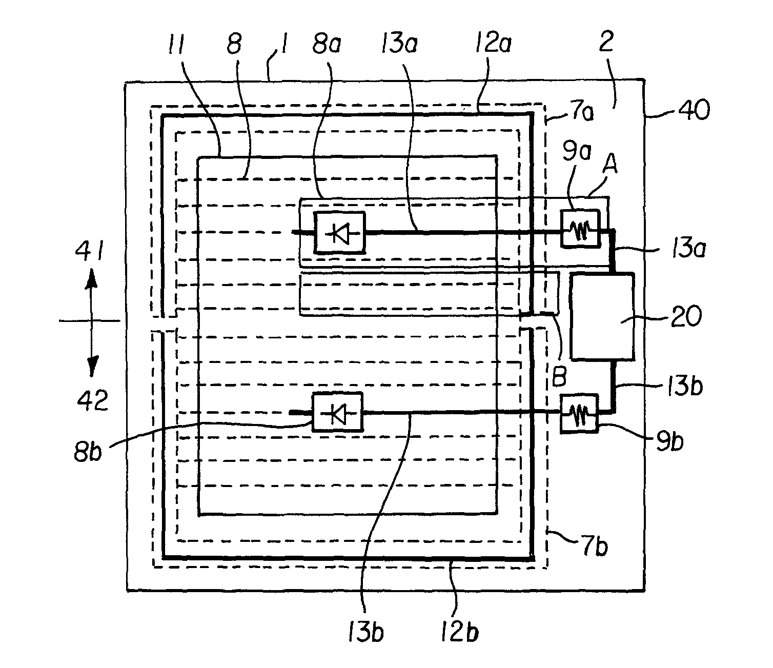
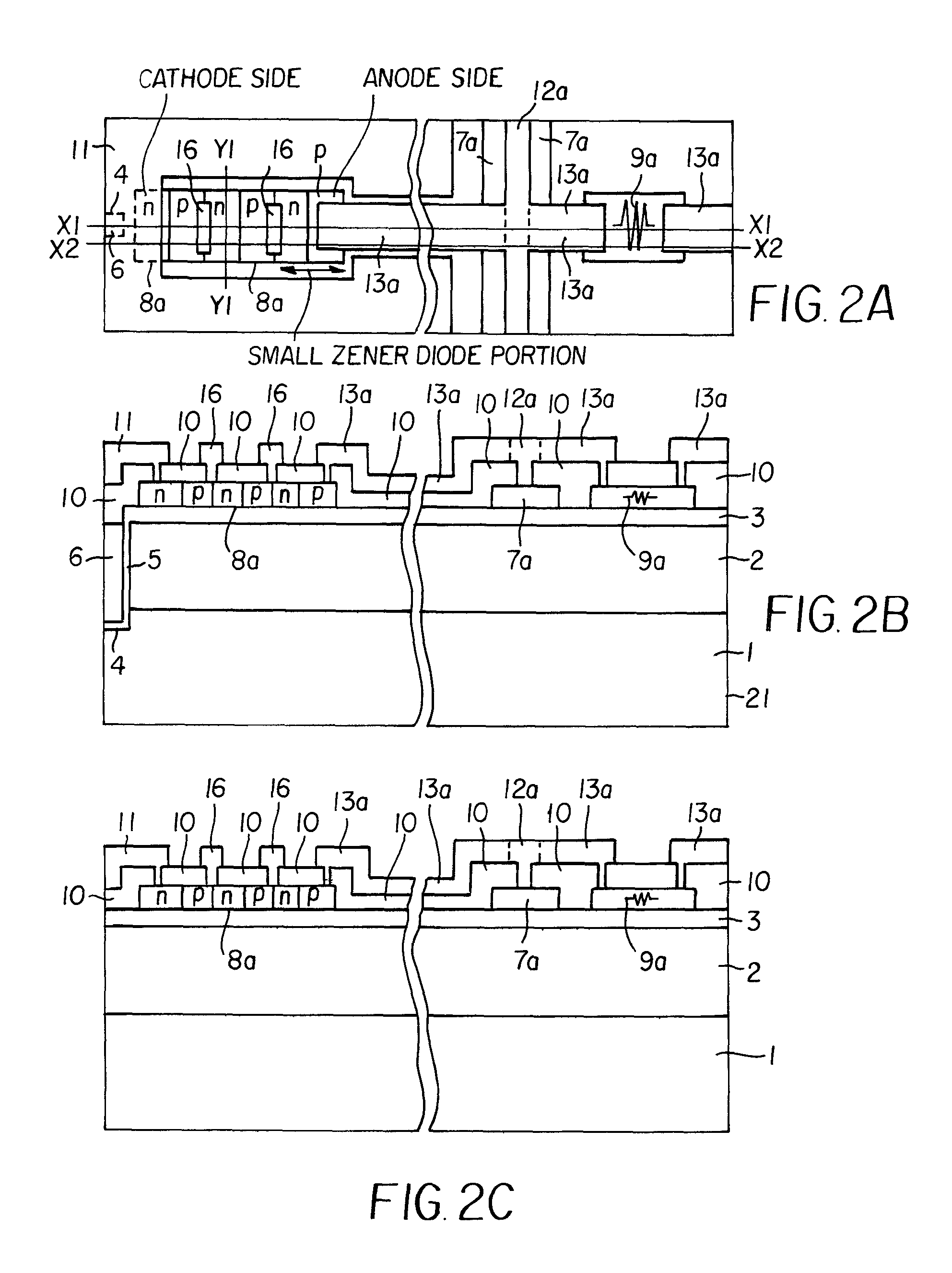
[0056]FIGS. 1, 2A to 2C, 3A to 3C, 4A and 4B are configuration views of a semiconductor device according to Embodiment 1 of the invention. FIG. 1 is a plan view schematically showing an important part of the semiconductor device. FIG. 2A is a detailed view of a portion A in FIG. 1. FIG. 2B is a sectional view of an important part, taken along the line X1-X1 in FIG. 2A. FIG. 2C is a sectional view of an important part, taken along the line X2-X2 in FIG. 2A. FIG. 3A is a detailed view of a portion B in FIG. 1. FIG. 3B is a sectional view of an important part, taken along the line X3-X3 in FIG. 3A. FIG. 3C is a sectional view of an important part, taken along the line X4-X4 in FIG. 3A. FIG. 4A is a sectional view of an important part, taken along the line Y1-Y1 in FIG. 2A. FIG. 4B is a sectional view of an important part, taken along the line Y2-Y2 in FIG. 3A. Description will be made here in the case where a trench gate type IGBT is taken as an example.
[0057]The semiconductor device i...
embodiment 2
[0077]FIG. 8 is an equivalent circuit diagram of a semiconductor device according to Embodiment 2 of the invention. The point of difference from FIG. 1 lies in that Zener diodes are connected to each other back-to-back. In FIG. 1, the backward withstand voltage of each Zener diode reaches several hundred V or more because each Zener diode is composed of a large number of series-connected Zener diode parts. For this reason, when a high backward surge voltage is applied to a gate of an IGBT, the IGBT is broken down. When Zener diodes 8c and 8d each having the same number of series-connected Zener diode parts as those of Zener diodes 8a and 8b, and Zener diodes 8a and 8b are back-to-back connected as shown in FIG. 8 to protect each IGBT from breakdown, an excessive backward voltage is prevented from being applied to the gate of the IGBT, so that the IGBT can be prevented from breakdown.
[0078]Zener diodes 8c and 8d may be formed simultaneously with the Zener diodes 8a and 8b.
embodiment 3
[0079]FIG. 9 is a plan view of important part of a semiconductor device according to Embodiment 3 of the invention. The point of difference from FIG. 1 lies in that one Zener diode 8 and one polysilicon resistor 9 are formed in a chip 40.
[0080]Embodiment 3 becomes effective for a module having a large number of chips 40 disposed therein as described with reference to FIG. 16. Also in this case, equalization of temperatures among the chips can be attained because the gate voltage of high-temperature chip 40 is reduced to throttle a current flowing in high-temperature chip 40.
PUM
 Abstract
Description
Claims
Application Information