

Solar cell wherein solar photovolatic thin film is directly formed on base
a solar photovolatic and solar cell technology, applied in the field of solar cell without solar energy, can solve the problems of thin film solar cell durability, cost, power generation efficiency,
- Summary
- Abstract
- Description
- Claims
- Application Information
AI Technical Summary
Benefits of technology
Problems solved by technology
Method used
Image

Examples
embodiment 1
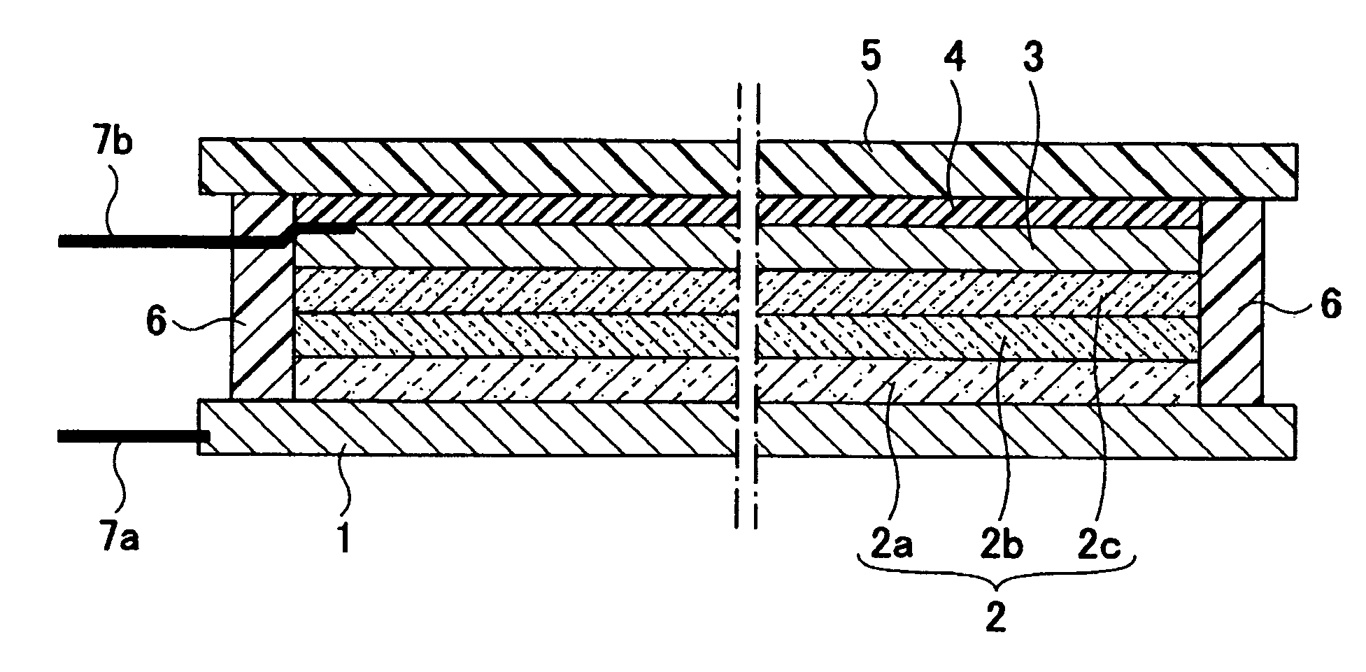
[0055]1. Base 1
[0056]Material: Aluminum plate, Thickness: approximately 5 mm (there is approximately 50 μm surface unevenness)
[0057]Process: A cleansing process after a sand blasting process
[0058]Furthermore, the oxide film is removed by plasma as described below. Ar: 1SLM and H: 100 sccm are passed to one-step shower plate type microwave excitation high-density-plasma apparatus (refer to non-patent literature 1). By supplying 3 kW of microwave power, H radical is generated efficiently and H radical mainly removes the oxide of aluminum and surface moisture.
[0059]In addition, it is also possible to remove oxide of aluminum (Al) and surface moisture by passing Ar: 1 SLM from the upper row shower plate of two-step shower plate type microwave excitation high-density-plasma apparatus (non-patent literature 1), applying RF power (13.56 MHz) of approximately 100 volts onto the substrate (susceptor) as substrate bias and irradiating ion in plasma. At this time, other noble gas may be used i...
embodiment 2
[0106]1. Base 1
[0107]Material: Steel plate Thickness 5 mm zinc / aluminum plating
[0108]Process: A cleansing process after zinc / aluminum plating process
[0109]2. N-Type Semiconductor Thin Film 2a
[0110]The same as Embodiment 1.
[0111]3. I-Type Semiconductor Thin Film 2b
[0112]The same as Embodiment 1.
[0113]4. P-Type Semiconductor Thin Film 2c
[0114]The same as Embodiment 1.
[0115]5. Transparent electrode film 3
[0116]Material: ITO thickness 1 μm
[0117]Process: PVD under 100 mTorr: Reactive sputtering of Ar / O2 (noble gas / O2) is performed by targeting ITO.
[0118]6. Moisture Diffusion-Preventing Film 4
[0119]The same as embodiment 1.
[0120]7. Transparent protective plate 5
[0121]Material: Transparent wired glass Thickness 3 mm
[0122]Process: Adherent (the transparent protective plate 5 is attached with urethane resin as a sealing agent 6 so that the semiconductor thin film 2 (2a, 2b, 2c), the transparent electrode film 3, and the moisture diffusion-preventing film 4 may be sealed).
[0123]8. Electrod...
embodiment 3
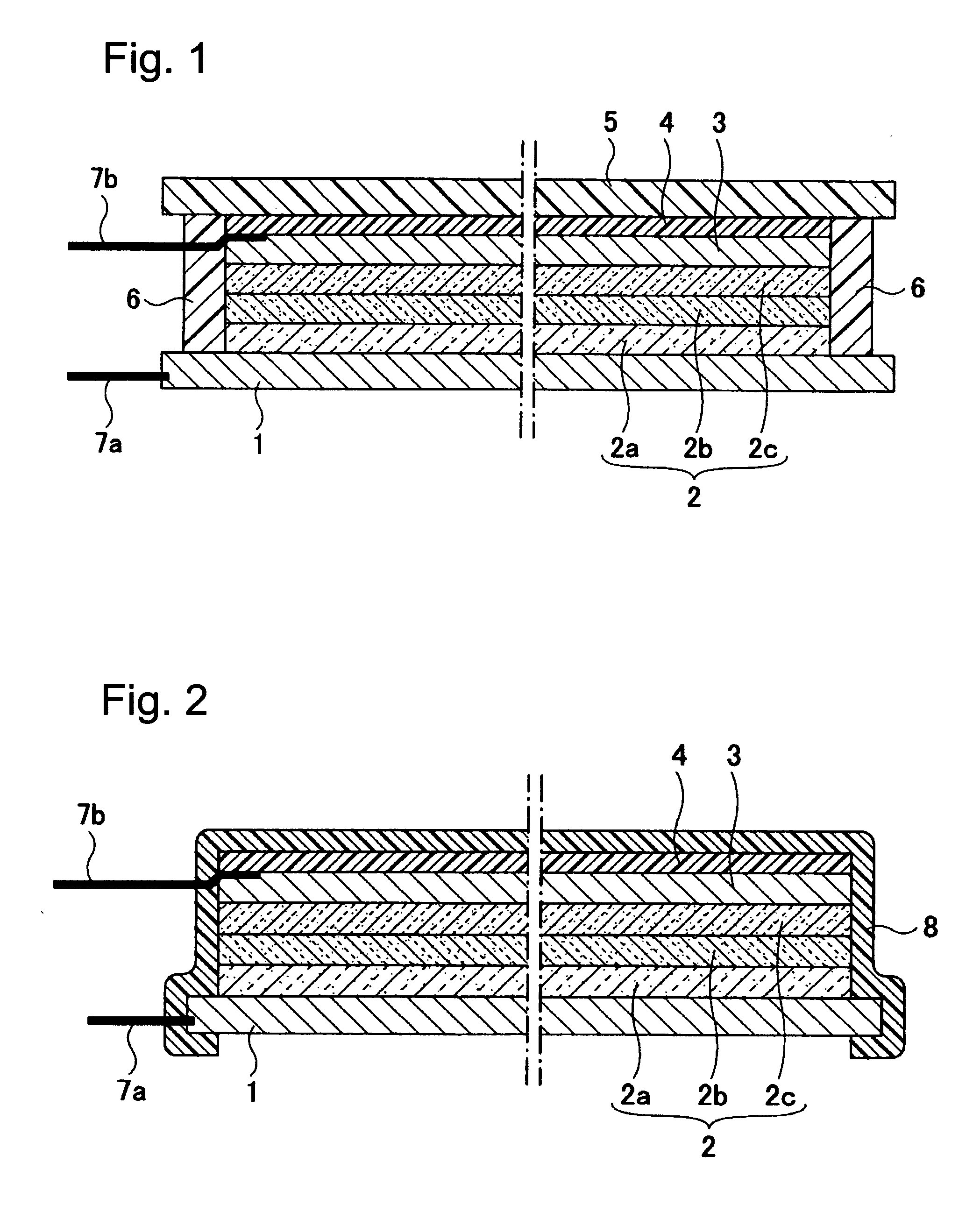
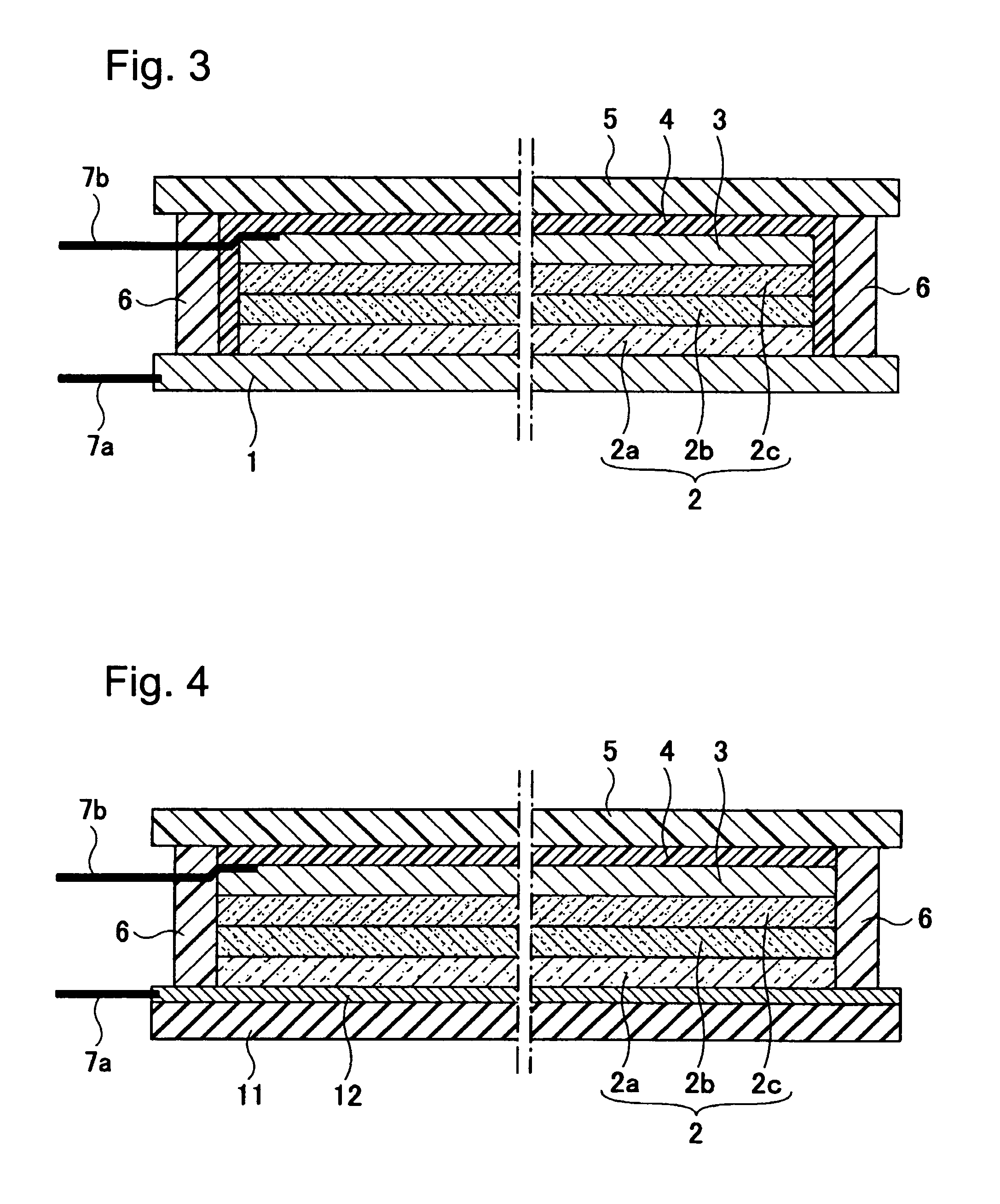
[0128]1. Base 11
[0129]Material: Ceramic tile, Thickness, 15 mm (a metal conducting film is put onto the surface)
[0130]Process: Wash the surface of the base and form an aluminum film (metal conducting film 12) on the washed surface by a spraying process.
[0131]Cleansing process: The same as Embodiment 1.
[0132]2. N-Type Semiconductor Thin Film 2a
[0133]The same as Embodiment 1.
[0134]3. I-Type Semiconductor Thin Film 2b
[0135]The same as Embodiment 1.
[0136]4. P-Type Semiconductor Thin Film 2c
[0137]The same as Embodiment 1.
[0138]5. Transparent Electrode Film 3
[0139]The same as Embodiment 1.
[0140]6. Moisture Diffusion-Preventing Film 4
[0141]The same as Embodiment 1.
[0142]7. Transparent Protective Plate 5
[0143]Material: Clear glass Thickness 7 mm
[0144]Process: The same as Embodiment 1.
[0145]8. Electrode Material 7b (Positive Electrode)
[0146]The same as Embodiment 1.
[0147]9. Electrode Material 7a (Negative Electrode)
[0148]Material: Resin covered copper wire
[0149]Process: Soldering (the abo...
PUM
| Property | Measurement | Unit |
|---|---|---|
| temperature | aaaaa | aaaaa |
| transparent conductive | aaaaa | aaaaa |
| non-conductive | aaaaa | aaaaa |
Abstract
Description
Claims
Application Information