Electron emitting element and method for producing electron emitting element

a technology of electron emitting element and electron emitting device, which is applied in the manufacture of electrode systems, discharge tubes luminescnet screens, instruments, etc., can solve the problems of oxidizing various substances, breaking down of electron emitting elements, and ozone being harmful to human bodies, etc., to achieve stable electron emission characteristic, facilitate electricity flow, and facilitate formation

Active Publication Date: 2010-12-30
SHARP KK
View PDF43 Cites 23 Cited by
  • Summary
  • Abstract
  • Description
  • Claims
  • Application Information

AI Technical Summary

Benefits of technology

[0019]In the configuration of the electron emitting element of the present invention, while a voltage is applied between the electrode substrate and the thin-film electrode, current flows in the electron acceleration layer and a part of electrons in the current becomes ballistic electrons due to an intense electric field formed by the voltage thus applied, thereby causing the ballistic electrodes to be emitted from a side of the thin-film electrode.
[0020]The electrons are emitted from an electron emitting section that is formed in advance in the electron acceleration layer positioned below the thin-film electrode, not from unprescribed portions on the side of the thin-film electrode. The electron emitting section is an exit of a conductive path, which is provided in the electron acceleration layer so as to run through the electron acceleration layer in a thickness direction of the electron acceleration layer. The electrons to be emitted from the thin-film electrode are supplied to the thin-film electrode via the conductive path and then emitted to outside from the thin-film electrode.
[0021]Such a conductive path (a conductive path formed in advance) can be easily formed by a forming process in the atmosphere, due to action of a single material or a mixed material which is provided in a fine particle layer containing insulating fine particles and which facilitates electricity flow in a thickness direction of the fine particle layer.
[0022]The forming process in the atmosphere is a process of applying a direct voltage between the electrode substrate and the thin-film electrode in the atmosphere, so as to form a conductive path for current in the element that flows from a side of the electrode substrate toward a side of the thin-film electrode via the fine particle layer
[0023]Since the conductive path is formed in advance in the electron acceleration layer by the forming process in the atmosphere as such, even if a voltage is subsequently applied

Problems solved by technology

This causes a problem of breakdown of the electron emitting element due to sputtering.
Ozone is harmful to human bodies, and oxidizes various substances because of its strong oxidizing power.
This causes a problem

Method used


Image

  • Electron emitting element and method for producing electron emitting element
  • Electron emitting element and method for producing electron emitting element
  • Electron emitting element and method for producing electron emitting element

Examples


embodiments 1 , 2

Embodiments 1, 2

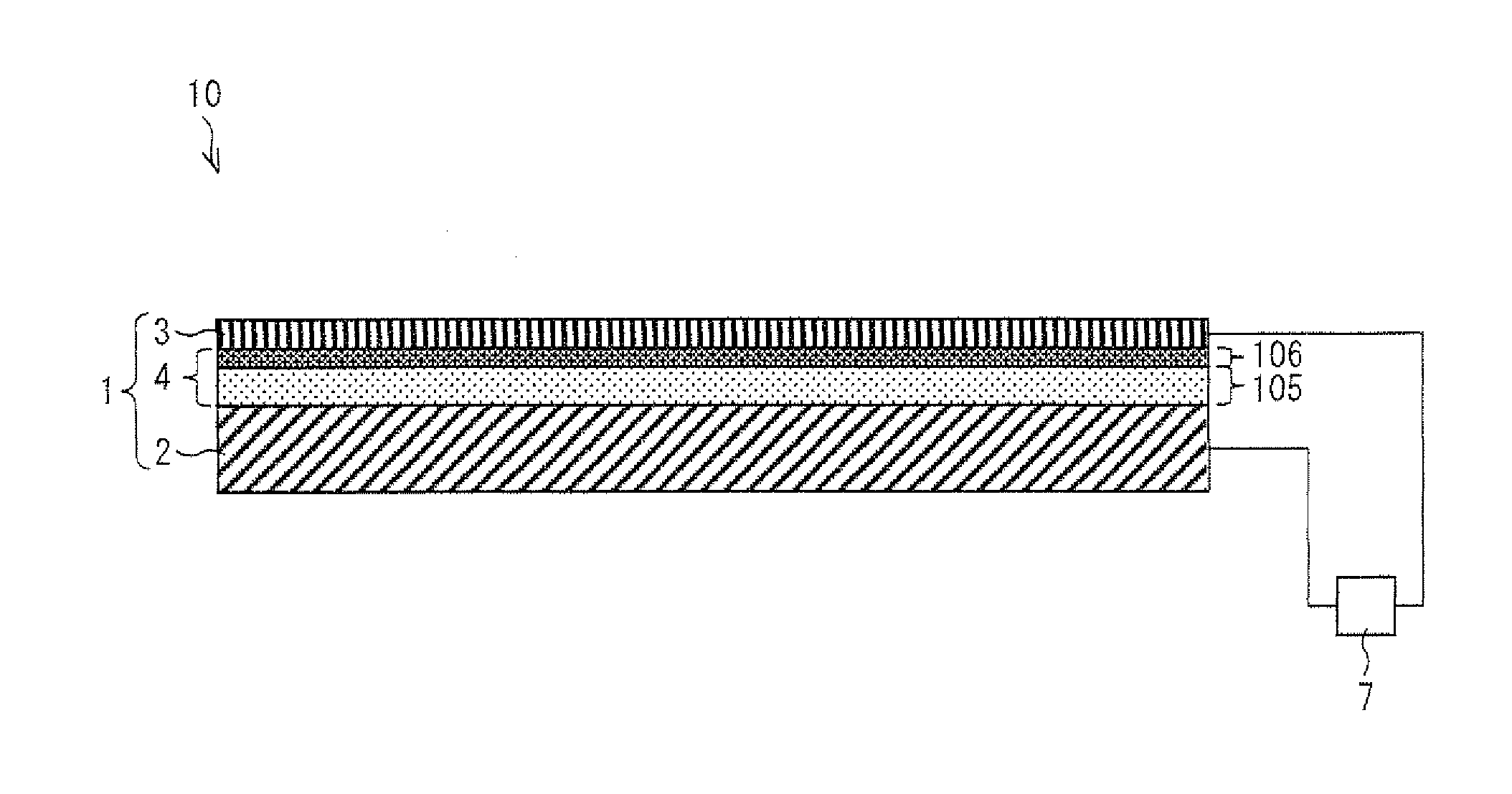
[0061]FIG. 1 is a schematic view illustrating a configuration of an electron emitting device 10 including an electron emitting element 1 according to one embodiment of the present invention.

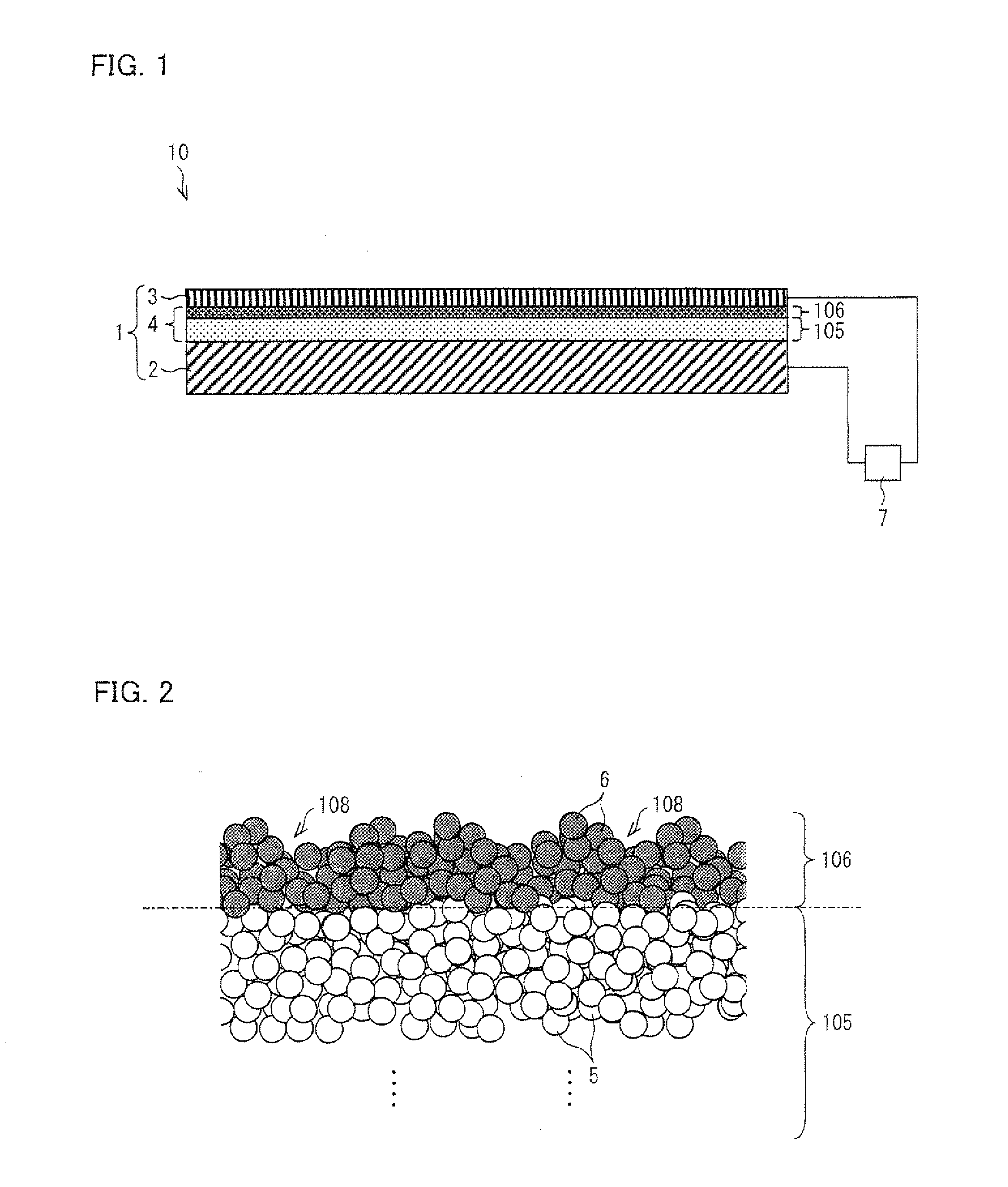
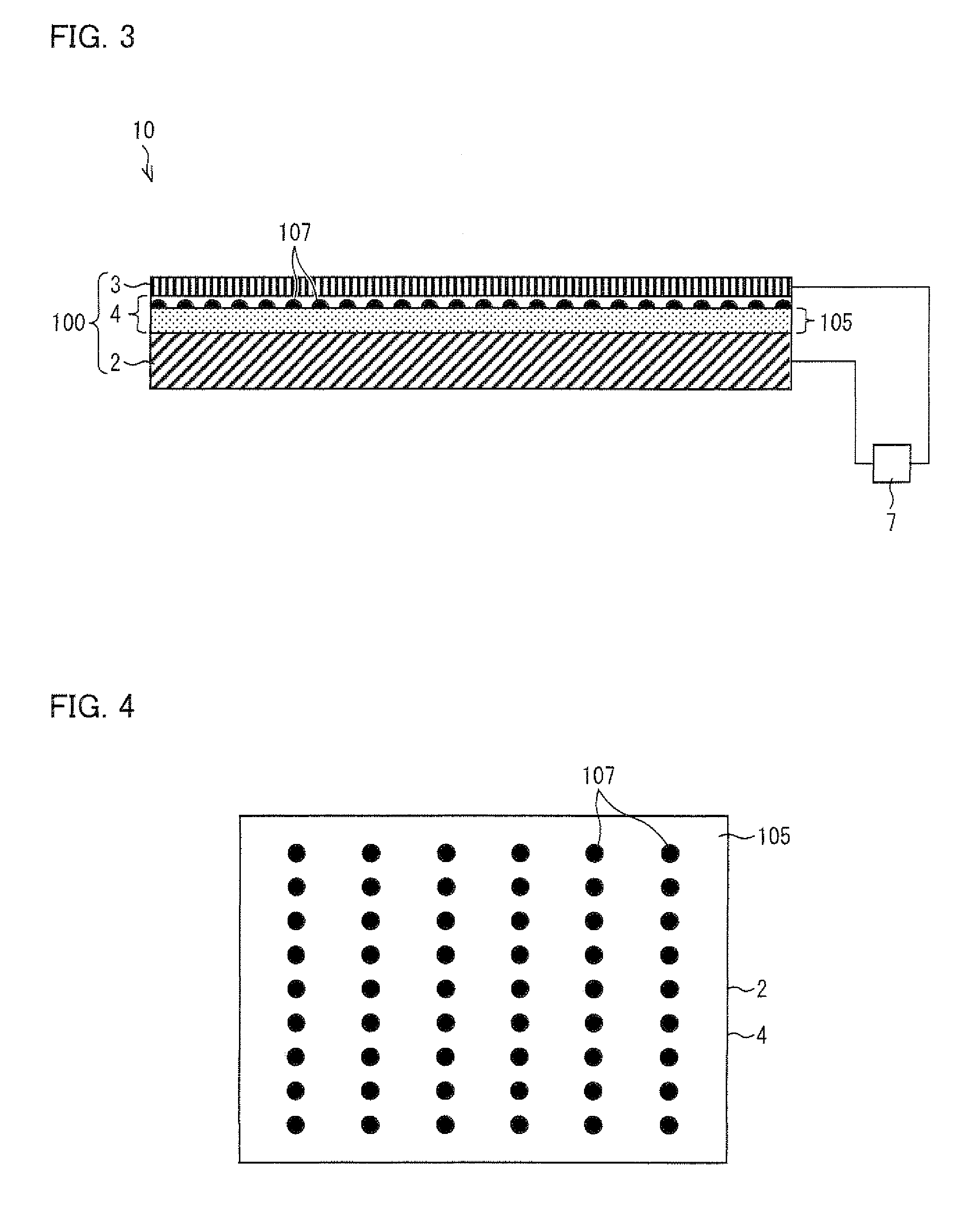
[0062]As illustrated in FIG. 1, the electron emitting device 10 includes an electron emitting element 1 according to one embodiment of the present invention, and a power supply 7. The electron emitting element 1 includes: an electrode substrate 2 as a bottom electrode; a thin-film electrode 3 as an upper electrode; and an electron acceleration layer 4 sandwiched therebetween. The power supply 7 applies a voltage between the electrode substrate 2 and the thin-film electrode 3.

[0063]While the voltage is applied between the electrode substrate 2 and the thin-film electrode 3, current flows in the electrode acceleration layer 4 sandwiched between the electrode substrate 2 and the thin-film electrode 3. A part of electrons in the current is emitted from the electron acceleration layer ...

example 1

[0144]Into a 10-mL reagent bottle, 2.0 g of an ethanol solvent and 0.5 g of tetramethoxysilane KBM-04 (manufactured by Shin-Etsu Chemical Co., Ltd.) were added. Further, as insulating fine particles 5, 0.5 g of spherical silica particles AEROSIL R8200 (manufactured by Evonik Degussa Japan Co., Ltd.) having an average diameter of 12 nm were added to the reagent bottle, and the reagent bottle was set in an ultrasonic dispersion device, so as to obtain an insulating fine particle dispersion solution A.

[0145]Then, the insulating fine particle dispersion solution A was dropped onto a 25 mm-square glass substrate having an ITO thin film on its surface, as the electrode substrate 2, and the glass substrate was subjected to spin-coating at 8000 rpm and 10 s so as to form a silica particle layer as the fine particle layer 105. Then, the glass substrate was dried at a room temperature for a few hours.

[0146]Subsequently, a tetradecane dispersion solution (manufactured by ULVAC, Inc., an averag...

example 2

[0157]As Example 2, an electron emitting element of Sample #2 was formed almost in the same procedure as in Example 1, except that the basic solution was not applied to the silica particle layer having a number of silver-particle domes. In Example 2, in the atmospheric forming process, a crack or a split could be formed in a silver-particle dome and electron emission in vacuum could be observed. However, it was difficult to control current flowing in the element and to control a degree of the crack or the split formed in the silver-particle dome.


PUM


Abstract

An electron emitting element includes an electrode substrate, a thin-film electrode, and an electron acceleration layer provided between them. The electron acceleration layer includes a fine particle layer containing insulating fine particles, which is provided on a side of the electrode substrate, and a deposition of conductive fine particles, which is provided on a surface of the fine particle layer. In the electron acceleration layer, a conductive path is formed in advance, and the deposition has a physical recess which is an exit of the conductive path and which serves as an electron emitting section. Electrons are emitted via the electron emitting section. With the arrangement, it is possible to realize an electron emitting element which prevents that an electrode on an electron emission side gradually wears off along with electron emission and which can maintain an electron emission characteristic for a long period.

Description

[0001]This Nonprovisional application claims priority under U.S.C. §119(a) on Patent Applications No. 2009-151559 filed in Japan on Jun. 25, 2009 and No. 2009-151561 filed in Japan on Jun. 25, 2009, the entire contents of which are hereby incorporated by reference.TECHNICAL FIELD[0002]The present invention relates to an electron emitting element, a method for producing the electron emitting element, an electron emitting device, a light emitting device, and an image display device.BACKGROUND ART[0003]A Spindt-type electrode and a carbon nanotube electrode (CNT) have been known as conventional electron emitting elements. Applications of such conventional electron emitting elements to, for example, the field of Field Emission Display (FED) have been studied. Such electron emitting elements are caused to emit electrons by tunnel effect resulting from formation of an intense electric field of approximately 1 GV / m that is produced by application of a voltage to a pointed section.[0004]How...

Claims


Application Information

Patent Timeline
IPC IPC(8): H01J1/02H01J9/02
CPCB82Y10/00H01J63/02H01J1/312G02F2001/133625G02F1/133625
Inventor HIRAKAWA, HIROYUKINAGAOKA, AYAEIMURA, YASUOIWAMATSU, TADASHI
Owner SHARP KK
Why Eureka
Try Eureka