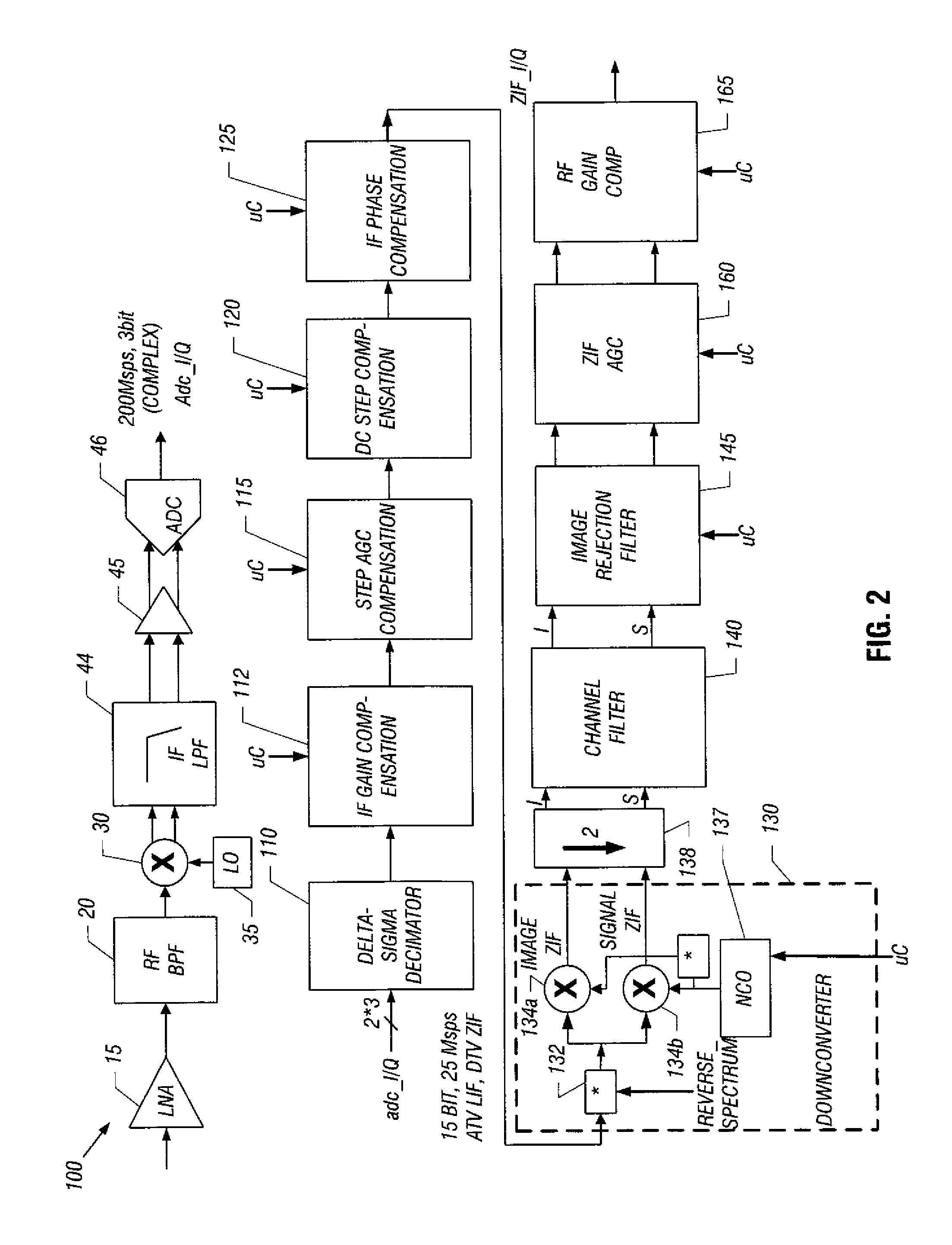
[0007]A digital configurable DC step compensation circuit can be coupled to the output of the step AGC compensation circuit to provide fine overall control of the mixed-
signal path DC offset when used in conjunction with relatively coarse analog
gain steps with associated coarse DC offset steps. This step circuit can also be configured by the MCU, and may receive a timing signal by which application of the DC offset changes may be synchronized to the coarse analog
gain adjustment and further synchronized to some predetermined desirable location in the ATV waveform. A digital IF
phase compensation circuit can be coupled to the output of the DC step compensation circuit and be configured by the MCU according to predetermined IF analog
phase response characteristics. Also provided in some embodiments may be a configurable spectrum reversal circuit, allowing optional performance of the function Y(
Omega)=X(−
Omega). The MCU may configure this circuit according to predetermined conditions, such as the expected orientation of the TV signal within the spectrum of the received channel. In addition, many of the above-described functions can be reordered (to the extent that they all operate on the channel located at a low IF input frequency), where tradeoffs in order can be made for efficiency.
[0008]A configurable digital downconverter may perform a complex
frequency shift of the desired channel. The value of the
frequency shift can be determined by the MCU according to a predetermined
frequency plan and may be responsive to a dynamic
automatic frequency control (AFC)
algorithm calculated by the MCU. The downconverter may further perform the complementary
frequency shift of the image channel. In some embodiments, a
decimation block coupled to the signal and image outputs of the downconverter may reduce sampling rate, permitting fewer calculations in downstream
signal processing blocks which may reduce device
power consumption, RF interference, and die area. In one embodiment, a configurable dual-channel real-valued
channel filter can be coupled to and operate on the two complex outputs of the decimator, configured by the MCU according to the expected channel bandwidth of the desired signal.
[0009]Then a
digital image rejection filter, coupled to the
channel filter outputs can minimize correlation between signal and image channels, thereby correcting circuit mismatches in the separate I and Q IF paths in the analog front-end. This filter may have parameters configured by the MCU and may be manipulated according to a determination of the magnitude of such mismatch as measured and reported to the MCU by the image rejection filter block. In turn, a configurable digital ZIF AGC block can be coupled to the output of the image rejection filter to optimize the digital word width and strategically locate the level of the resulting output within the
dynamic range of its reduced bit-width digital word, and which can be controlled by a
gain control signal configured by the MCU according to various
signal level measurements and characteristics of the desired channel. The gain
control signal can be applied to the signal path based on a timing signal, allowing synchronization to one or more predetermined desirable locations in the signal waveform.
[0014]Then, a collection of
digital signal processing blocks including a complex
frequency shifter, an FIR filter, and an AGC block incorporating a
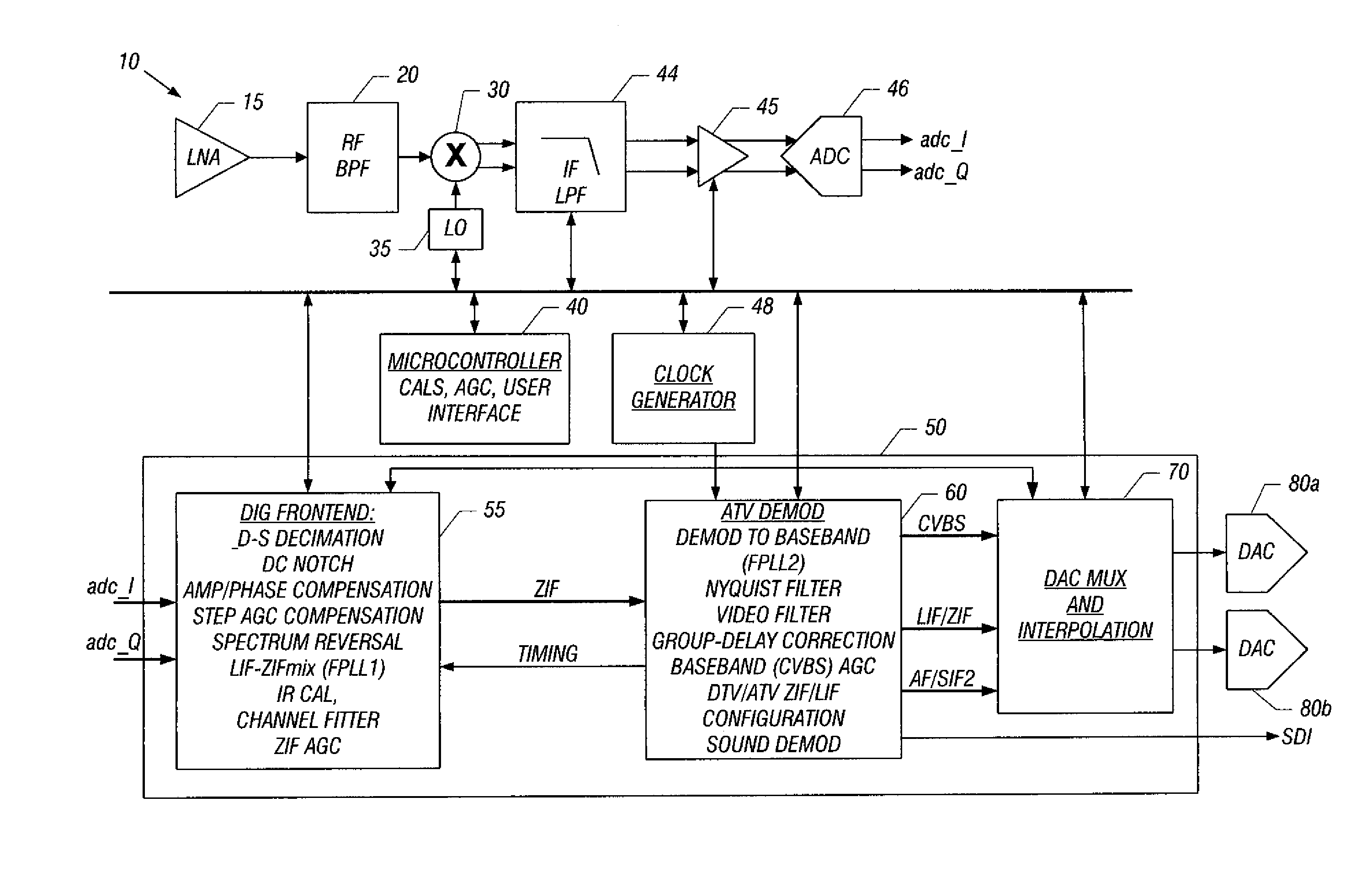
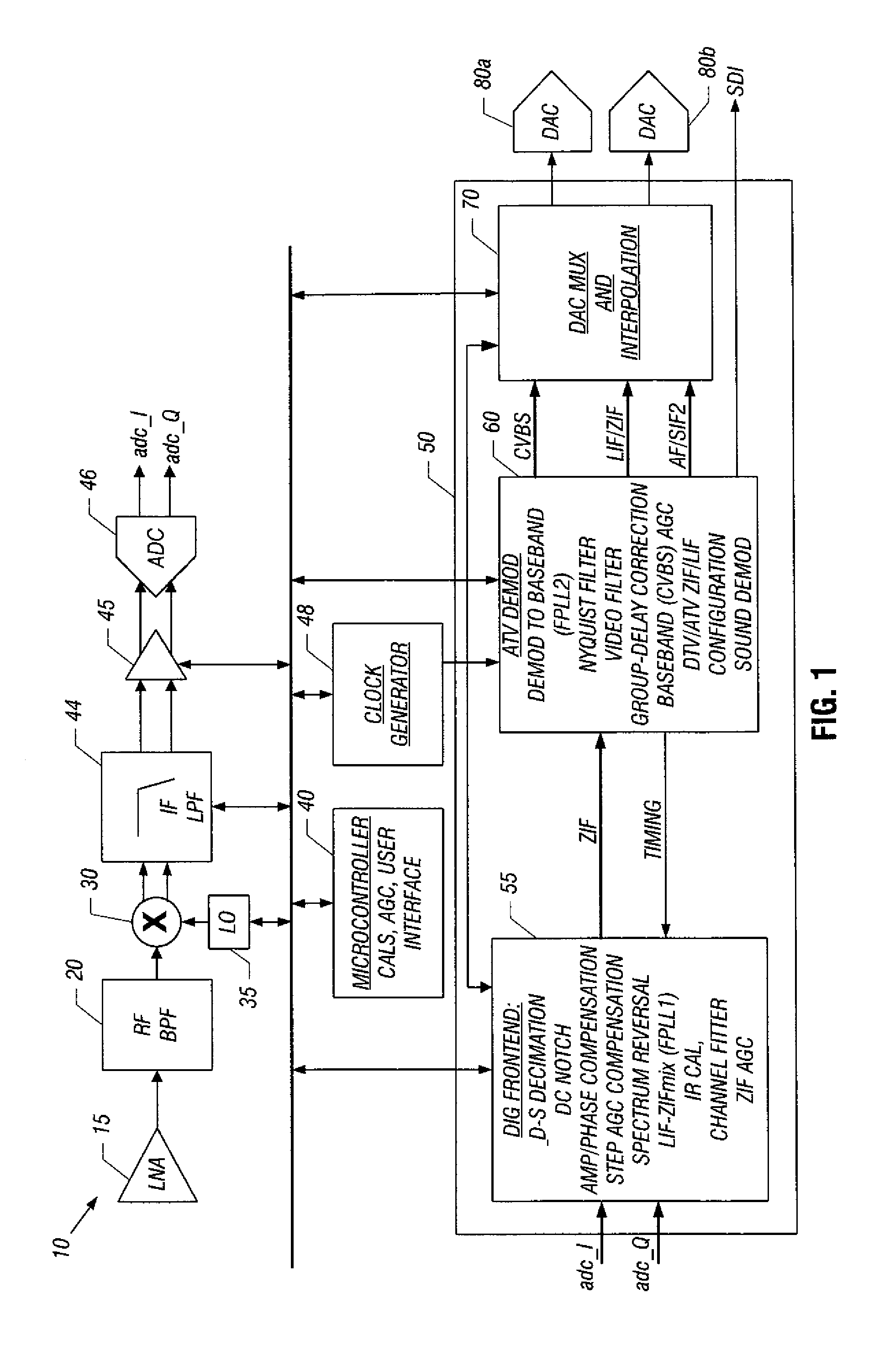
signal level detector and gain control under MCU control, can be selectively applied as components in a television sound demodulator or alternatively as final frequency translation and level adjustment operations on the signal path for a LIF ATV or DTV operating mode. In turn, a digital DAC
multiplexer and interpolation block can be coupled to the demodulated CVBS, the sound demodulator output, and the LIF tuner output signals, the input source of which is configured by the MCU according to device operating mode to select the type of data presented on the output through a pair of DAC's and to increase the sampling rate to a frequency high enough to make in-band distortions at the DAC outputs negligible. In some implementations, a
serial digital interface (SDI), coupled to the output of this block, can transmit the output signals to circumvent the DAC outputs, thereby eliminating a
noise source and a drain on power. Also, a serial communications link, such as an I2C link, may enable the user of the device to communicate with the MCU to establish operating mode and desired signal expectations.


