Inducing stress in CMOS device

a technology of cmos and stress liner, which is applied in the direction of semiconductor devices, electrical devices, transistors, etc., can solve problems such as adversely affecting device performan

Active Publication Date: 2011-01-13
ELPIS TECH INC
View PDF6 Cites 2 Cited by
  • Summary
  • Abstract
  • Description
  • Claims
  • Application Information

AI Technical Summary

Benefits of technology

Solutions for inducing stress in a complimentary metal oxide semiconductor (CMOS) device are disclosed. In one aspect, a method of forming a semiconductor device is disclosed, the method comprising: providing a CMOS device including: a silicon substrate layer; a silicon dioxide layer thereover; and an n-type field effect transistor (NFET) gate having a first recessed source / drain trench and a p-type field effect transistor (PFET) gate having a second recessed source / drain trench, the NFET gate and the PFET gate located over the silicon dioxide layer; depositing a nitride stress liner in the first recessed source / drain trench and the second recessed source / drain trench; depositing an oxide layer over the nitride stress liner; placing the CMOS device on a handling wafer, wherein the oxide layer is closest to the handling wafer; removing the silicon substrate layer; etching the silicon dioxide layer to form an opening abutting a portion of a source / drain region, the source / drain region abutting one of the first recessed source / drain trench or the second recessed source / drain trench; and forming a contact in the opening.
A first aspect of the invention provides a method of forming a semiconductor device, the method comprising: providing a complimentary metal oxide semiconductor (CMOS) device including: a silicon substrate layer; a silicon dioxide layer thereover; and an n-type field effect transistor (NFET) gate having a first recessed source / drain trench and a p-type field effect transistor (PFET) gate having a second recessed source / drain trench, the NFET gate and the PFET gate located over the silicon dioxide layer; depositing a nitride stress liner in the first recessed source / drain trench and the second recessed source / drain trench; depositing an oxide layer over the nitride stress liner; placing the CMOS device on a handling wafer, wherein the oxide layer is closest to the handling wafer; removing the silicon substrate layer; etching the silicon dioxide layer to form an opening abutting a portion of a source / drain region, the source / drain region abutting one of the first recessed source / drain trench or the second recessed source / drain trench; and forming a contact in the opening.
A second aspect of the invention provides a semiconductor device comprising: a silicon dioxide layer; an n-type field effect transistor (NFET) including at least one recessed source / drain trench and located over a portion of the silicon dioxide layer; a p-type field effect transistor (PFET) including at least one recessed source / drain trench and located over a portion of the silicon dioxide layer; a nitride stress liner over the NFET and the PFET, the nitride stress liner filling the at least one recessed source / drain trench of the NFET and the at least one recessed source / drain trench of the PFET; and a first contact formed in the silicon dioxide layer, the first contact abutting one of the NFET or the PFET.
A third aspect of the invention provides a semiconductor device comprising: a silicon dioxide layer; an n-type field effect transistor (NFET) including at least one recessed source / drain trench and located over a portion of the silicon dioxide layer; a p-type field effect transistor (PFET) including at least one recessed source / drain trench and located over a portion of the silicon dioxide layer; a first spacer abutting the NFET and a second spacer abutting the PFET; a nitride stress liner over the NFET and the PFET, the nitride stress liner filling the at least one recessed source / drain trench of the NFET and the at least one recessed source / drain trench of the PFET; and a first contact formed in the silicon dioxide layer, the first contact abutting one of the NFET or the PFET.

Problems solved by technology

However, stress liners located near device channels may cause complications during contact formation, and may adversely affect device performance.

Method used


Image

  • Inducing stress in CMOS device
  • Inducing stress in CMOS device
  • Inducing stress in CMOS device

Examples


Embodiment Construction

As used herein, the term “deposition” may include any now known or later developed techniques appropriate for the material to be deposited including but are not limited to, for example: chemical vapor deposition (CVD), low-pressure CVD (LPCVD), plasma-enhanced CVD (PECVD), semi-atmosphere CVD (SACVD) and high density plasma CVD (HDPCVD), rapid thermal CVD (RTCVD), ultra-high vacuum CVD (UHVCVD), limited reaction processing CVD (LRPCVD), metalorganic CVD (MOCVD), sputtering deposition, ion beam deposition, electron beam deposition, laser-assisted deposition, thermal oxidation, thermal nitridation, spin-on methods, physical vapor deposition (PVD), atomic layer deposition (ALD), chemical oxidation, molecular beam epitaxy (MBE), plating, evaporation, etc.

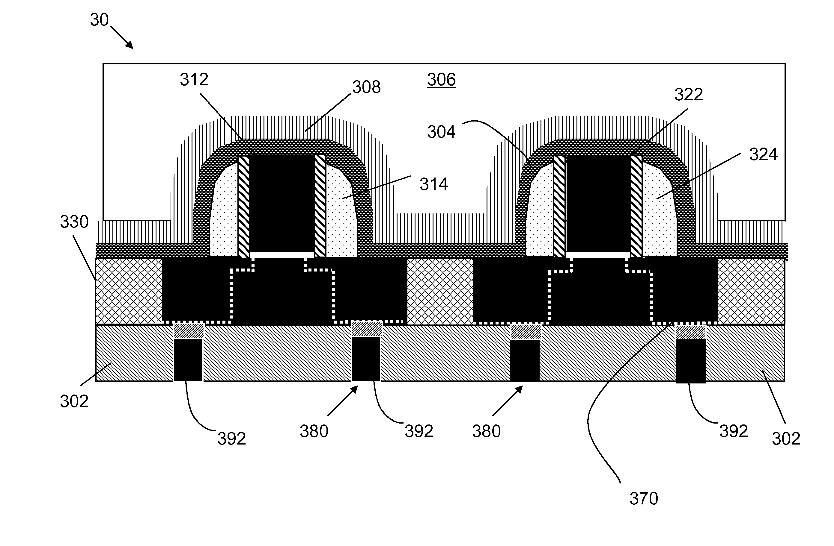
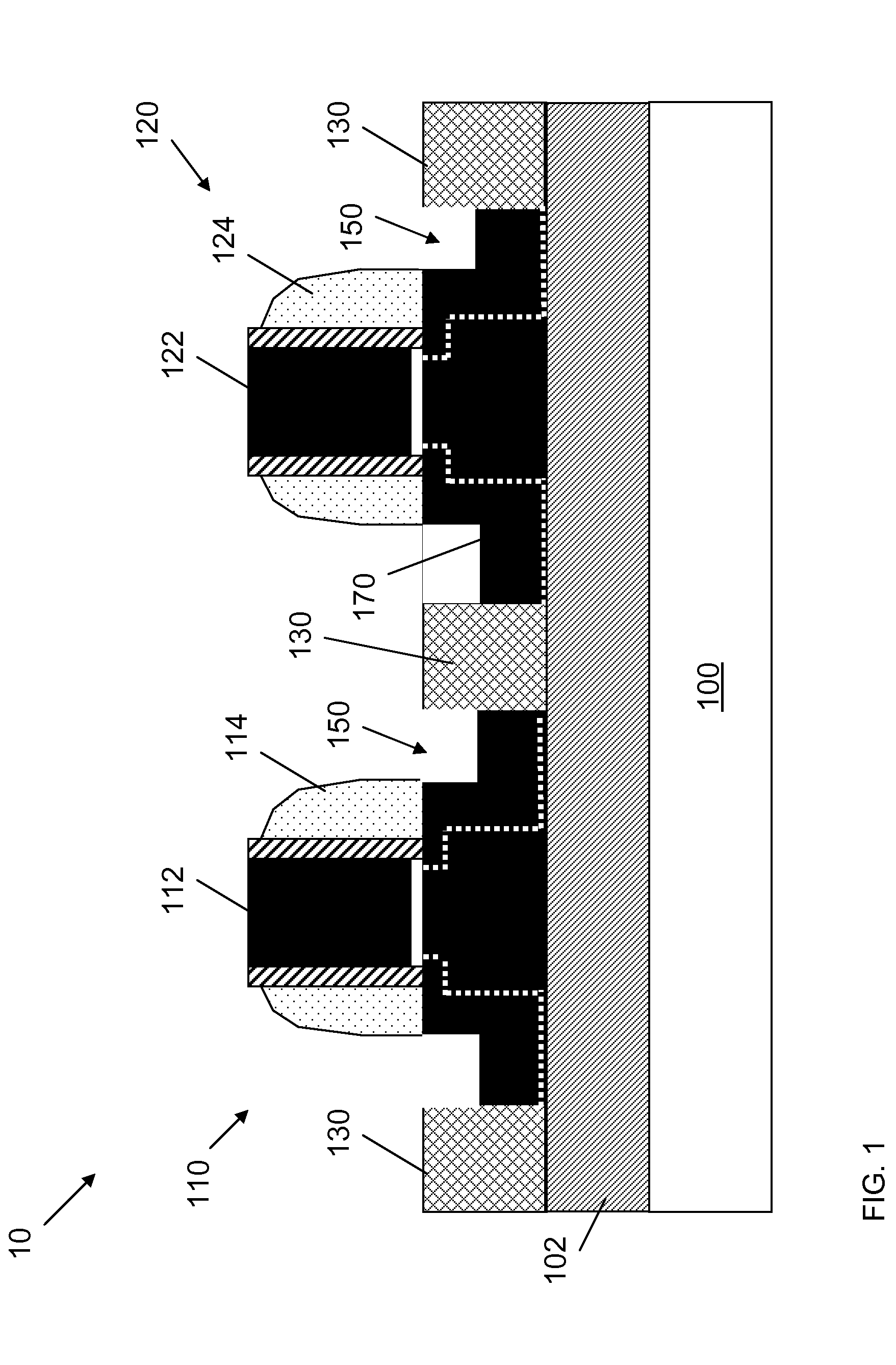
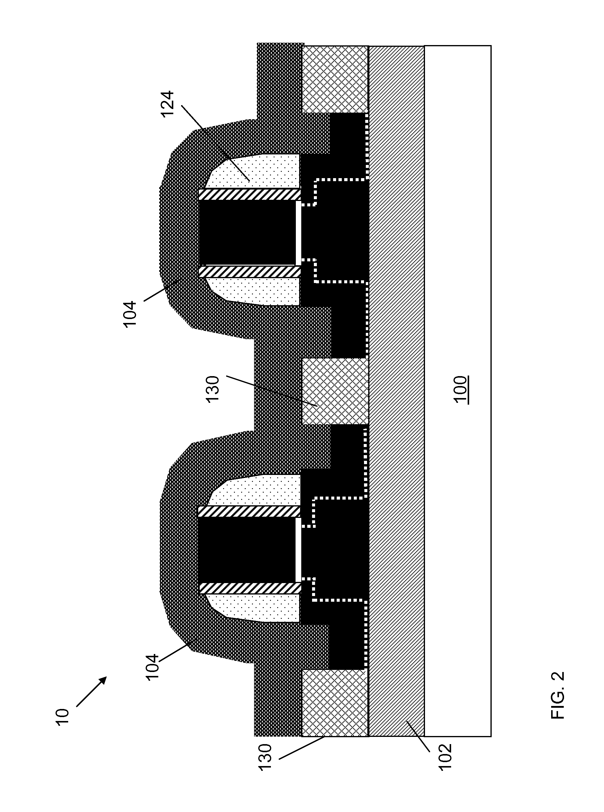
Turning to the figures, a method of forming a semiconductor device is shown in FIGS. 1-8. In particular, a method of forming a nitride stress liner over a complementary metal oxide semiconductor (CMOS) device is shown. FIG. 1 shows a co...


PUM


Abstract

A first aspect of the invention provides a method of forming a semiconductor device, the method comprising: providing a complimentary metal oxide semiconductor (CMOS) device including: a silicon substrate layer; a silicon dioxide layer thereover; and an n-type field effect transistor (NFET) gate having a first recessed source/drain trench and a p-type field effect transistor (PFET) gate having a second recessed source/drain trench, the NFET gate and the PFET gate located over the silicon dioxide layer; depositing a nitride stress liner in the first recessed source/drain trench and the second recessed source/drain trench; depositing an oxide layer over the nitride stress liner; placing the CMOS device on a handling wafer, wherein the oxide layer is closest to the handling wafer; removing the silicon substrate layer; etching the silicon dioxide layer to form an opening abutting a portion of a source/drain region, the source/drain region abutting one of the first recessed source/drain trench or the second recessed source/drain trench; and forming a contact in the opening.

Description

BACKGROUND OF THE INVENTIONThe subject matter disclosed herein relates to solutions for inducing stress in a Complementary Metal Oxide Semiconductor (CMOS). More specifically, the subject matter disclosed herein relates to systems and methods for forming a nitride stress liner in a CMOS device.Semiconductor device designers continually work to make semiconductor devices smaller while increasing their level of performance. One approach to increasing performance is the use of stress liners over portions of these devices. Stress liners may be particularly helpful, for example, in increasing electron / hole mobility in device channels. However, stress liners located near device channels may cause complications during contact formation, and may adversely affect device performance.BRIEF DESCRIPTION OF THE INVENTIONSolutions for inducing stress in a complimentary metal oxide semiconductor (CMOS) device are disclosed. In one aspect, a method of forming a semiconductor device is disclosed, the...

Claims


Application Information

Patent Timeline
Patent Type & Authority Applications(United States)
IPC IPC(8): H01L27/092H01L21/8238
CPCH01L21/823807H01L21/823814H01L21/823871H01L29/7848H01L27/1203H01L29/7843H01L21/84
Inventor LUO, ZHIJIONGLIANG, QINGQINGYIN, HAIZHOUZHU, HUILONG
Owner ELPIS TECH INC
Why Eureka
Try Eureka