Engineered interconnect dielectric caps having compressive stress and interconnect structures containing same

a dielectric cap and dielectric technology, applied in the field of integrated circuit chips, can solve the problems of copper diffused easily into the surrounding dielectric material, the scale of the device no longer meets requirements, and the inability to meet the requirements of aluminum, etc., to achieve the effect of high mechanical and electrical stability

Active Publication Date: 2011-01-20
GLOBALFOUNDRIES US INC
View PDF16 Cites 17 Cited by
  • Summary
  • Abstract
  • Description
  • Claims
  • Application Information

AI Technical Summary

Benefits of technology

[0012]In one aspect of the invention, a dielectric capping layer that has a low dielectric constant of less than conventionally used silicon nitride and silicon carbon nitride, and a higher mechanical and electrical stability to UV and/or E

Problems solved by technology

While aluminum-based metallurgies have been the material of choice for use as metal interconnects in the past, aluminum no longer satisfies requirements as circuit density and speeds for IC chips increase and the scale of the devices decrease to nanometer dimensions.
One challenge to using copper-based metallurgies is that copper diffuses readily into the surrounding dielectric material as processing steps continue.
Moreover, UV exposure causes prior art capping layers to crack and an adhesion problem between the capping layer and the ultra low dielectric constant dielectric material may arise.
Any crack in the capping layer may lead to metallic diffusion into the ILD layer through the s

Method used


Image

  • Engineered interconnect dielectric caps having compressive stress and interconnect structures containing same
  • Engineered interconnect dielectric caps having compressive stress and interconnect structures containing same

Examples


Embodiment Construction

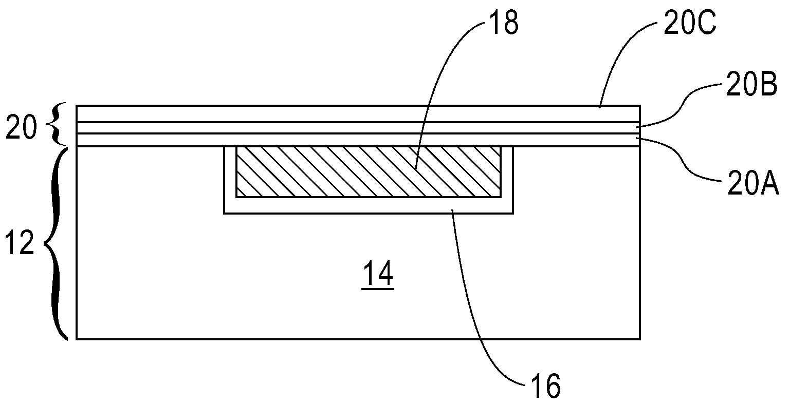
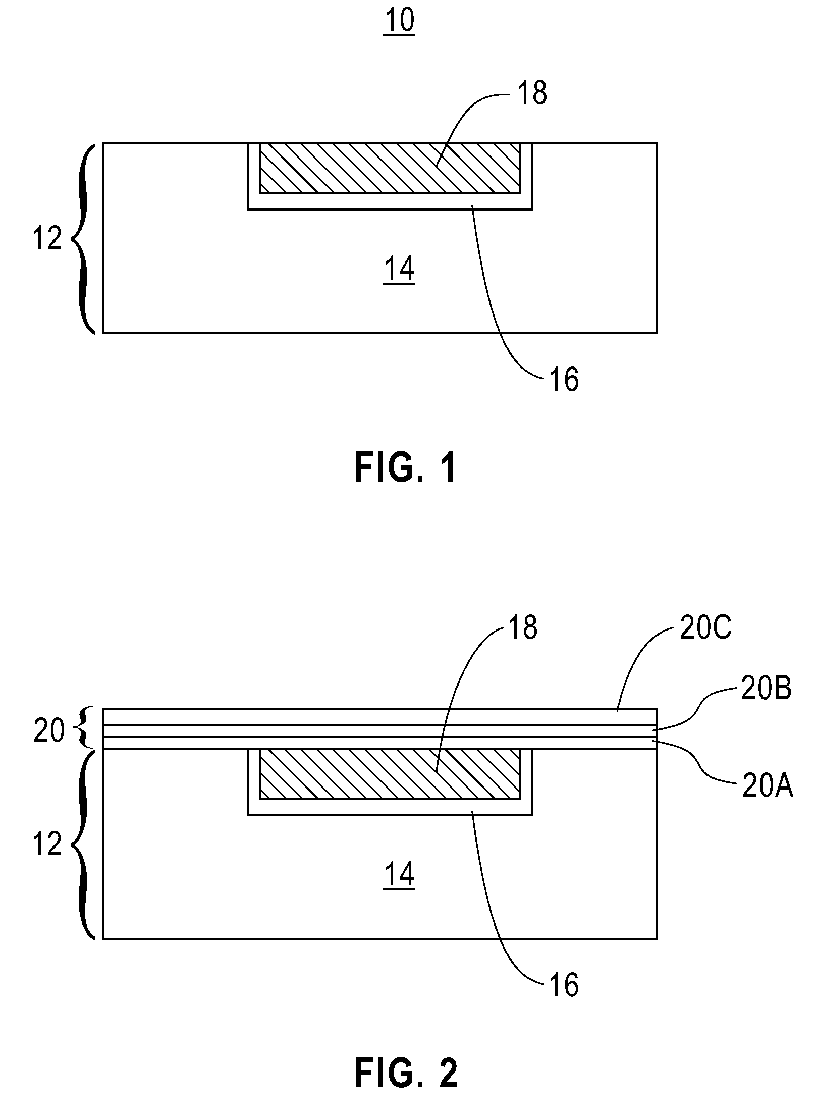
[0020]The present invention, which provides a dielectric capping layer having compressive stress even after post-deposition treatments, a method of fabricating the dielectric capping layer, and an interconnect structure including the dielectric capping layer, will now be described in greater detail by referring to the following discussion and drawings that accompany the present application. It is noted that the drawings of the present application are provided for illustrative purposes only and, as such, the drawings are not drawn to scale.

[0021]In the following description, numerous specific details are set forth, such as particular structures, components, materials, dimensions, processing steps and techniques, in order to provide a thorough understanding of the present invention. However, it will be appreciated by one of ordinary skill in the art that the invention may be practiced without these specific details. In other instances, well-known structures or processing steps have no...


PUM


Abstract

A dielectric capping layer having a dielectric constant of less than 4.2 is provided that exhibits a higher mechanical and electrical stability to UV and/or E-Beam radiation as compared to conventional dielectric capping layers. Also, the dielectric capping layer maintains a consistent compressive stress upon post-deposition treatments. The dielectric capping layer includes a tri-layered dielectric material in which at least one of the layers has good oxidation resistance, is resistance to conductive metal diffusion, and exhibits high mechanical stability under at least UV curing. The low k dielectric capping layer also includes nitrogen content layers that contain electron donors and double bond electrons. The low k dielectric capping layer also exhibits a high compressive stress and high modulus and is stable under post-deposition curing treatments, which leads to less film and device cracking and improved device reliability.

Description

BACKGROUND[0001]The present application relates generally to integrated circuit (IC) chips, and more particularly to a dielectric cap for use with a back-end-of-the-line (BEOL) interconnect structure, especially a BEOL interconnect structure including Cu embedded within an ultra-low k dielectric constant dielectric material.[0002]Generally, semiconductor devices include a plurality of circuits which form an IC fabricated on a semiconductor substrate. A complex network of signal paths will normally be routed to connect the elements distributed on the surface of the semiconductor substrate. Efficient routing of these signals across the device requires the formation of multilevel or multilayered schemes, such as, for example, single and dual damascene interconnect structures. Within a typical interconnect structure, metal vias run perpendicular to the semiconductor substrate, while metal lines run parallel to the semiconductor substrate.[0003]In traditional interconnect structures, alu...

Claims


Application Information

Patent Timeline
IPC IPC(8): H01L29/06H01L23/532H01L21/314
CPCH01L21/76825H01L21/76832H01L21/76834H01L23/53295H01L23/53238H01L23/53266H01L23/5329H01L23/53223H01L2924/0002H01L2924/00
Inventor COHEN, STEPHAN A.GRILL, ALFREDHAIGH, JR., THOMAS J.LIU, XIAO H.NGUYEN, SON V.SHAW, THOMAS M.SHOBHA, HOSADURGA
Owner GLOBALFOUNDRIES US INC
Why Eureka
Try Eureka