
Method for producing soi substrate

Active Publication Date: 2011-01-20
SHIN ETSU CHEM IND CO LTD
View PDF10 Cites 5 Cited by
  • Summary
  • Abstract
  • Description
  • Claims
  • Application Information

AI Technical Summary

Benefits of technology

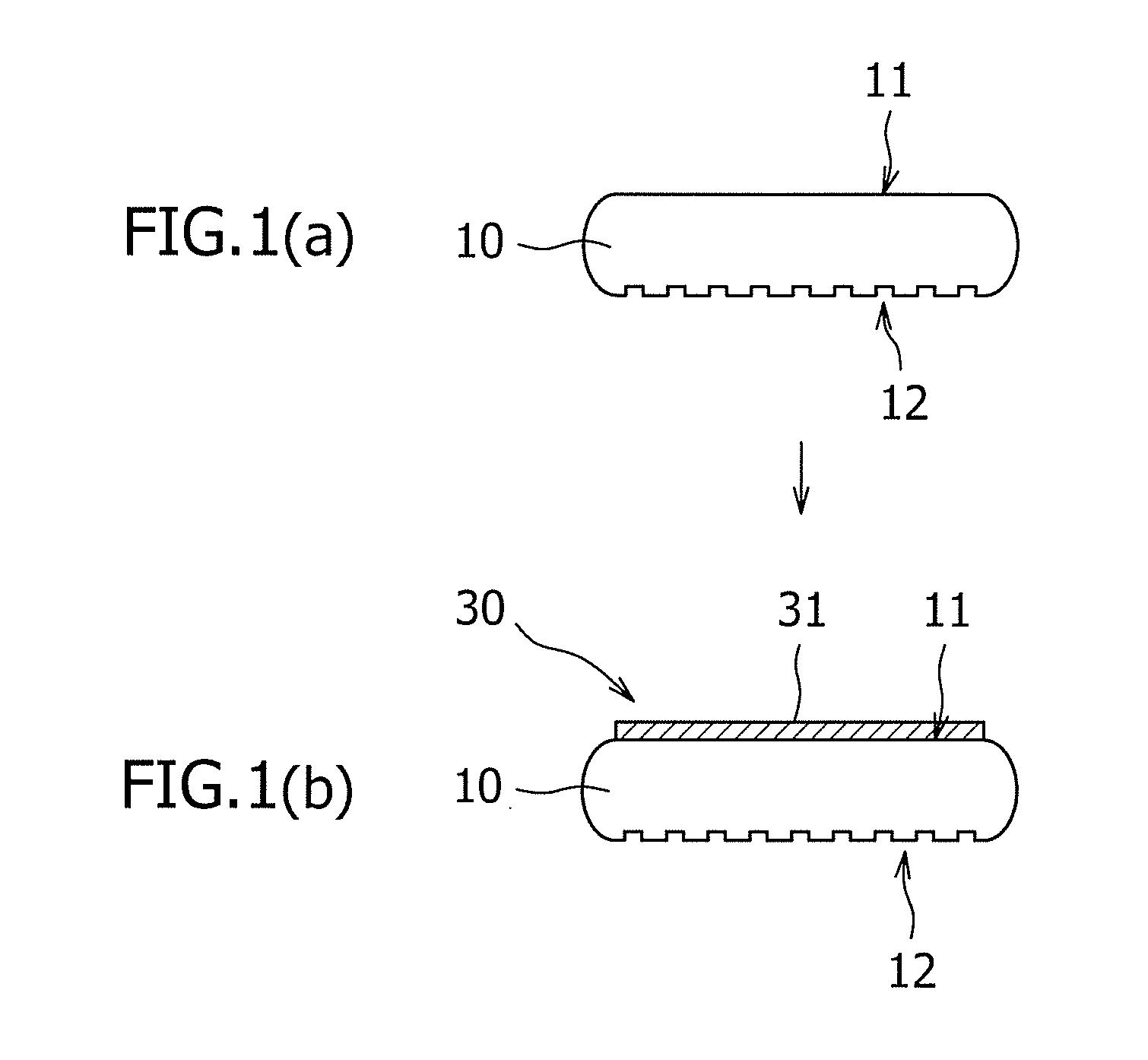
[0011]The present invention has been made in view of problems as described above. An object of the present invention is to provide a method for easily manufacturing an SOI substrate which comprises a transparent insulating substrate and a silicon film formed on a main surface of the substrate, while the other main surface thereof (an opposite to the main surface having the silicon film formed thereon) is roughened.
[0013]As described above, the method for manufacturing an SOI substrate comprising the steps of roughening and forming makes it possible to easily manufacture an SOI substrate comprising a transparent insulating substrate and a silicon film formed thereon and having a back surface (a main surface where the silicon film is not formed) roughened.
[0014]Moreover, according to the above SOI substrate, the back surface of the transparent insulating substrate has a high surface roughness, and scatters a signal from a recognition unit containing an optical sensor, thereby successfully preventing a problem that a substrate is not recognized with the recognition unit. Additionally, this helps to prevent slippage of the substrate during the conveyance, and the like.
[0015]According to a method for manufacturing an SOI substrate of the present invention, it is possible to easily manufacture an SOI substrate (transparent SOI substrate) comprising a transparent insulating substrate and a silicon film formed thereon and having a back surface (a main surface where the silicon film is not formed) roughened.
[0016]Moreover, according to the above SOI substrate, the back surface of the transparent insulating substrate has a high surface roughness, and scatters a signal from a recognition unit containing an optical sensor, thereby allowing the recognition unit to recognize the substrate. Additionally, this helps to prevent slippage of the substrate during the conveyance, and the like.

Problems solved by technology

Since the quartz substrate is transparent in the above bonded substrate, the bonded substrate may have different problems in process and evaluation from the problems of normal SOI substrates manufactured by bonding a silicon substrate to another silicon substrate.
One of such problems is that, when being conveyed on equipment, an SOI substrate including a silicon film formed on a transparent insulating substrate such as an SOQ substrate (hereinafter, sometimes abbreviated as a transparent SOI substrate) is unlikely to be recognized by an optical sensor for recognizing substrates, for example.
However, in the fields of electronic materials and devices, foggy surfaces formed by such a method have several problems.
One of them is a particle (foreign matter) problem.
This problem is caused by a sandblast powder remaining on a treated surface; dust generated from an acute portion, a crack and a damaged portion of a roughened surface; and so forth.
These problems cannot be solved by normal cleaning in many cases.
Moreover, a problem such as metal contamination attributable to this foreign matter is also serious in the field of electronic materials.
This particle problem can be critical particularly when a product treated by this fogging treatment is used in the field of semiconductor.
Additionally, there is a problem that particles on transparent substrates such as those of SOQ (Silicon on Quartz) and SOG (Silicon on Glass) significantly increase in amount when back surfaces of the transparent substrates are subjected to the fogging treatment for making the transparent substrates recognizable by substrate-recognition sensors of various apparatuses.
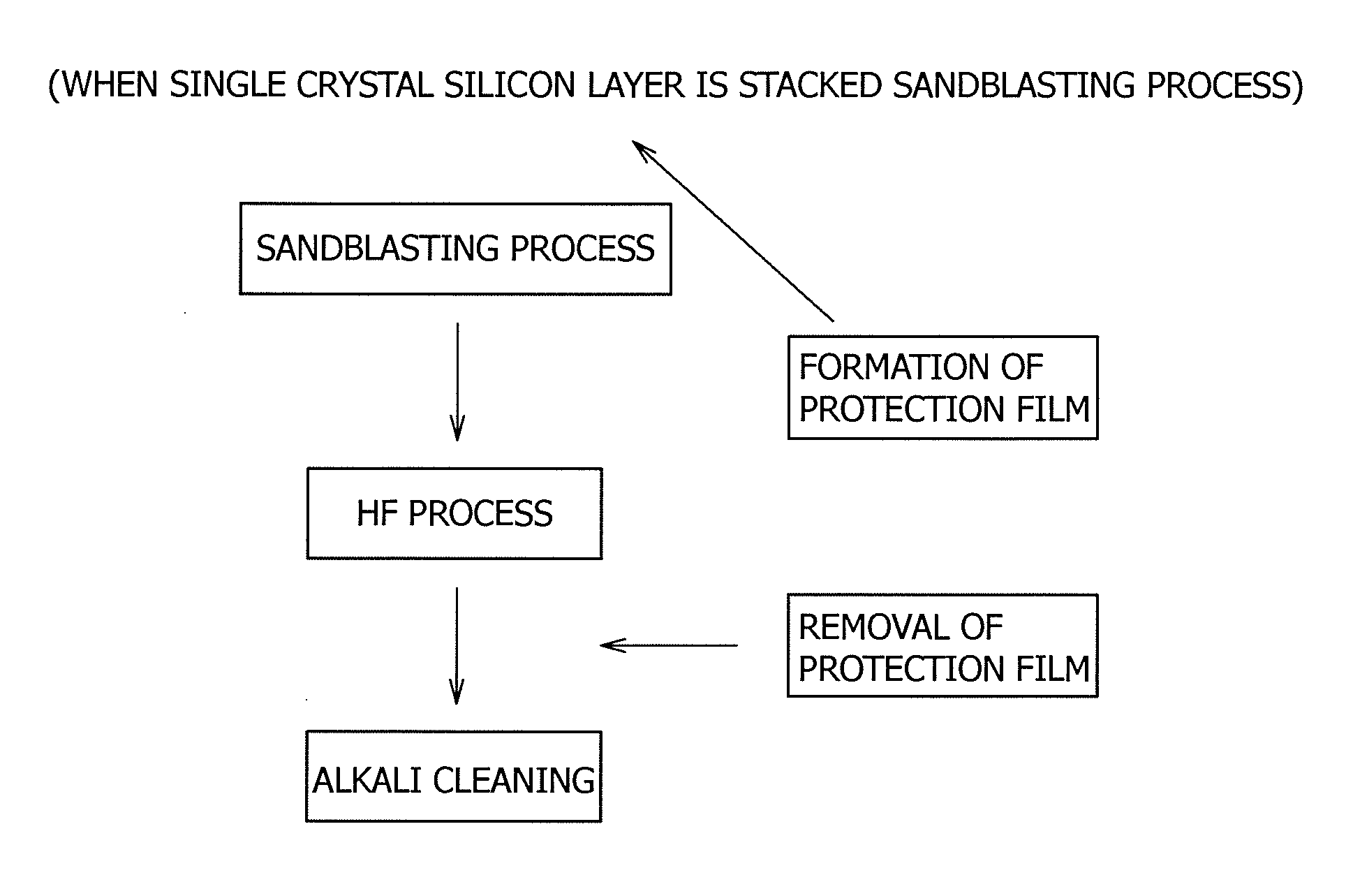
The HF cleaning, however, has a problem of making the particle level rather worse.
Furthermore, if the cleaning is performed for a long period with high concentration HF to remove the particles, the surface subjected to the fogging treatment is made excessively smooth, thereby decreasing the effect of roughing the surface.

Method used


Image

  • Method for producing soi substrate
  • Method for producing soi substrate
  • Method for producing soi substrate

Examples


example 1

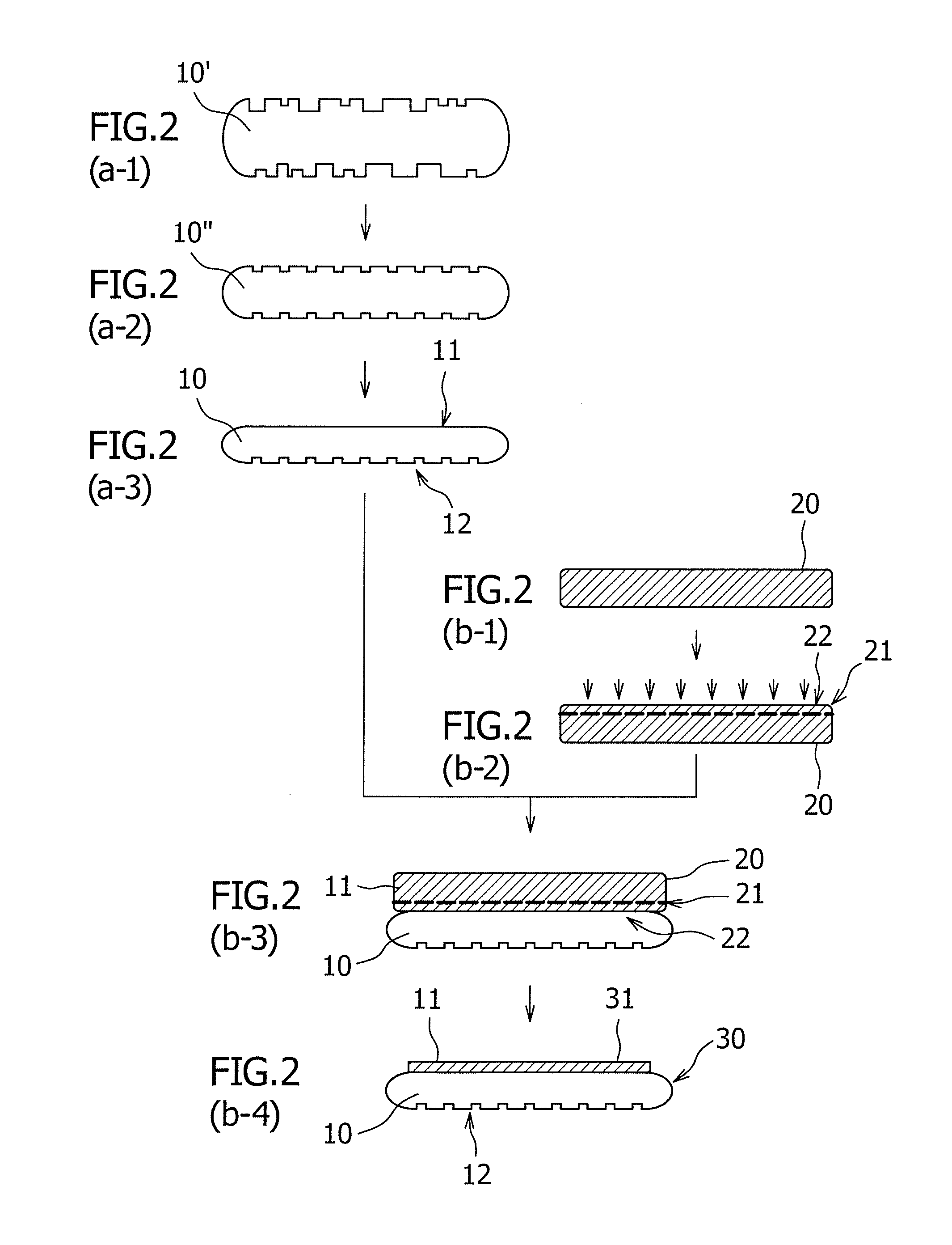
[0109]According to the method for manufacturing an SOI substrate by using a bonding method, as shown in FIG. 2, thirty transparent SOI substrates were manufactured as follows.

[0110]First, a synthetic quartz substrate 10′ having a diameter of 150 mm was prepared by being cut out directly from a synthetic quartz ingot (substep a-1).

[0111]Next, double-sided lapping was performed on both surfaces of this synthetic quartz substrate 10′ with a double-sided lapping machine, and etching was performed thereon using hydrofluoric acid (substep a-2). Then, the synthetic quartz substrate was annealed under a non-oxidizing atmosphere at 1100° C. for 30 minutes.

[0112]The synthetic quartz substrate 10″ had only one of the surfaces polished by using a one surface polisher. Thus, one main surface (first main surface) 11 had an RMS surface roughness of 0.2 nm (substep a-3). The other main surface (second main surface) 12 had an RMS surface roughness of 1.0 nm.

[0113]Next, a single crystal silicon subst...

examples 3 to 7

[0129]First, six quartz wafers were sandblasted.

[0130]Next, each two of the wafers were treated under each of the following conditions.

[0131]Example 3: the wafers were immersed in 2% by weight HF solution for 30 minutes, and subsequently immersed in 3% by volume NH4OH solution for 10 minutes.

[0132]Example 4: the wafers were immersed in 2% by weight HF solution for 30 minutes, and subsequently immersed in an alkali solution (NH4OH:H2O2:H2O=1:1:10 at weight ratio) for 10 minutes.

[0133]Example 5: the wafers were immersed in 2% by weight HF solution for 30 minutes, and subsequently immersed in an alkali solution (NH4OH:H2O2:H2O=1:0.2:10 at weight ratio) for 10 minutes.

[0134]Example 6: the wafers were immersed in 2% by weight HF solution for 30 minutes, and subsequently immersed in an alkaline organic solvent (8% TMAH solution) for 10 minutes.

[0135]Example 7: the wafers were immersed in 2% by weight HF solution for 30 minutes, and subsequently immersed in an alkali solution (10 wt% KOH s...


PUM


Abstract

A method for easily manufacturing a transparent SOI substrate having: a main surface with a silicon film formed thereon; and a rough main surface located on a side opposite to a side where the silicon film is formed. A method for manufacturing transparent SOI substrate, having a silicon film formed on a first main surface of the transparent insulating substrate, while a second main surface of the transparent insulating substrate, an opposite to the first main surface, is roughened. The method includes at least the steps of: roughening the first main surface with an RMS surface roughness lower than 0.7 nm and the second main surface with an RMS surface roughness higher than the surface roughness of the first main surface to prepare the transparent insulating substrate; and forming the silicon film on the first main surface of the transparent insulating substrate.

Description

BACKGROUND OF THE INVENTION[0001]1. Field of the Invention[0002]The present invention relates to a method for manufacturing an SOI substrate, and particularly relates to a method for manufacturing an SOI substrate in which a silicon film is formed on one main surface of a transparent insulating substrate.[0003]2. Description of Related Art[0004]In order to achieve higher performance of semiconductor devices, attention has been focused on SOI (silicon on insulator) substrates in recent years. Additionally, some types of SOI substrates such as a silicon on quartz (SOQ) substrate and a silicon on glass (SOG) substrate which have support substrates (handle wafers) made of non-silicon materials are also expected to be applied to TFT-LCDs, high-frequency (RF) devices, other MEMS products, and so forth (for example, see JP2006-324530A).[0005]There has been proposed a method for manufacturing the aforementioned SOQ substrate or the like, by using, for example, a silicon substrate for a dono...

Claims


Application Information

Patent Timeline
IPC IPC(8): H01L21/762
CPCH01L27/12H01L21/76254
Inventor AKIYAMA, SHOJIKAWAI, MAKOTOITO, ATSUOKUBOTA, YOSHIHIROTANAKA, KOUICHITOBISAKA, YUJITAMURA, HIROSHI
Owner SHIN ETSU CHEM IND CO LTD
Learn More