
Wave-guide coupling spr sensor chip and sensor chip array thereof

a sensor chip and waveguide technology, applied in the field of surface plasmon resonance (spr) detection methods, can solve the problems of low sensitivity of methods, difficult to actually apply lrspr to complex detection environments, and can only be excited, so as to achieve effective tuning, high interrogation precision, and tunable optical properties

Inactive Publication Date: 2011-02-17
THE NAT CENT FOR NANOSCI & TECH NCNST OF CHINA
View PDF5 Cites 25 Cited by
  • Summary
  • Abstract
  • Description
  • Claims
  • Application Information

AI Technical Summary

Benefits of technology

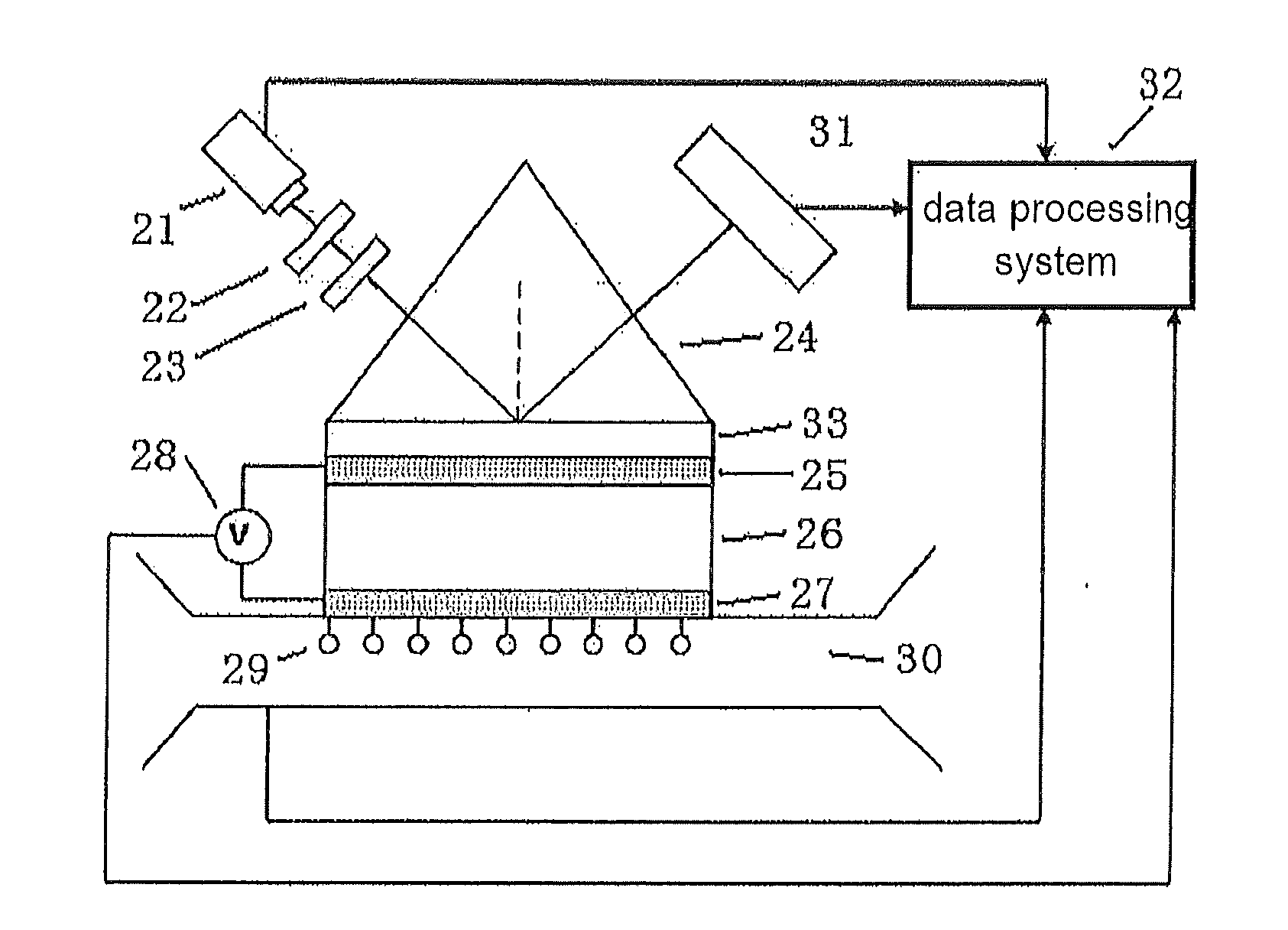
[0035]The above sensor chip further comprises a refractive index matching layer that is adapted to eliminate interference from air gap and to facilitate effective coupling of the light path. A material of the refractive index matching layer is refractive index matching liquid or refractive index matching film. The function of the refractive index matching layer is to effectively couple the incident light to the corresponding functional layers of the sensor and to eliminate the possible interference from the air gap present on the interface. The parameters, such as the material property and thickness of the refractive index matching layer, should not harm the WCSPR detection function of the sensor and the tuning function of the dielectric waveguide layer.
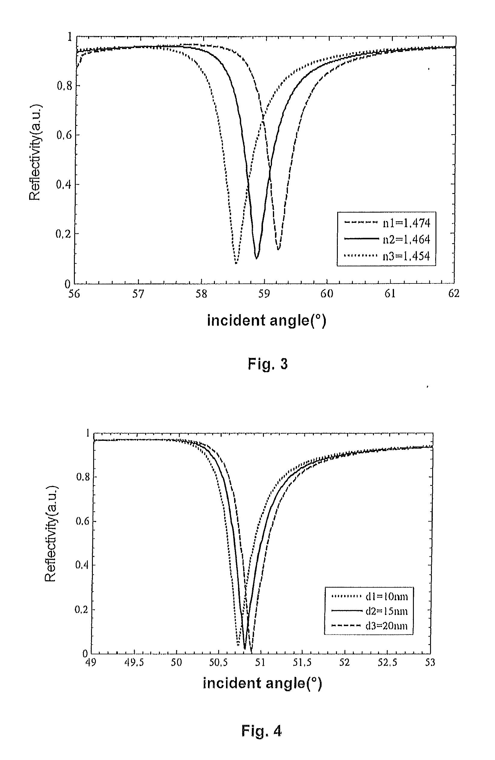
[0070]4. The tunable optical dielectric layer in the WCSPR detection structure according to the invention may be realized using the materials having the electro-optical effect (i.e., electrical intensity-related refractive index) or the thermo-optical effect (i.e., temperature-related refractive index) and other materials with changeable index of refraction. The material having the electro-optical effect includes, but is not limited to: inorganic electro-optical material (e.g., LiNbO3), organic / polymer electro-optical material, liquid crystal and the like; the material having the thermo-optical effect includes, but is not limited to, inorganic thermo-optical material (e.g., SiO2), organic thermo-optical polymer and the like, Comparing with inorganic crystal material, the organic / polymer electro-optical material has the advantages of low cost, being easy to process, higher response speed and higher non-linear coefficient (Advances in Polymer Science, 2002 □vol 158, Springer-Verlag Berlin Heidelberg).

Problems solved by technology

Unfortunately, the LPSRP can only be excited when the refractive indices of the dielectrics on both sides of the metal are similar.
As a result, it is not easy to actually apply the LRSPR to complicated detection environments.
However, this method suffers for low sensitivity.
However, the resulting apparatus will be too bulky and more vulnerable to the mechanical noise and thermal drift.
Moreover, the scanning speed of the system is very low due to the fact that the operational speed of the precise mechanical rotating table is limited.
Thus, it is difficult to realize fast real-time measurement with high time resolution.
Besides, the precise mechanical control rotating table needed for angular interrogation is of high maintenance cost and bulky volume, and frequent calibration is required.
Thereby, it is difficult for the angular interrogation to be used in compact and portable instruments.
Moreover, the cost for realizing high resolution with the method is very high; the volume of the involved device is hard to reduce and the scanning speed is limited.
However, the achieved detection sensitivity of the Intensity Interrogation is the lowest among the three methods, due to the limitation of the number of detectors used in the array.
Moreover, it is not suitable for high density multi-channel parallel detections.
In the above, several SPR detection structures and SPR signal interrogation methods are described in detail, from which it can be seen that the following problems have to be solved when the SPR is used as sensors, i.e., low precision and sensitivity, low system interrogation speed, bulky volume, and not being able to carry out high density multi-channel parallel detections.

Method used


Image

  • Wave-guide coupling spr sensor chip and sensor chip array thereof
  • Wave-guide coupling spr sensor chip and sensor chip array thereof
  • Wave-guide coupling spr sensor chip and sensor chip array thereof

Examples


Embodiment Construction

[0082]According to the invention, information on a detected sample is obtained by changing parameters of optical properties of the dielectric waveguide layer, using the WCSPR structure as the basic structure of sensing measurement. Thus, it is possible to implement SPR sensors with high resolution, SNR, and to improve response time and to realize large-scale multi-channel scanning.

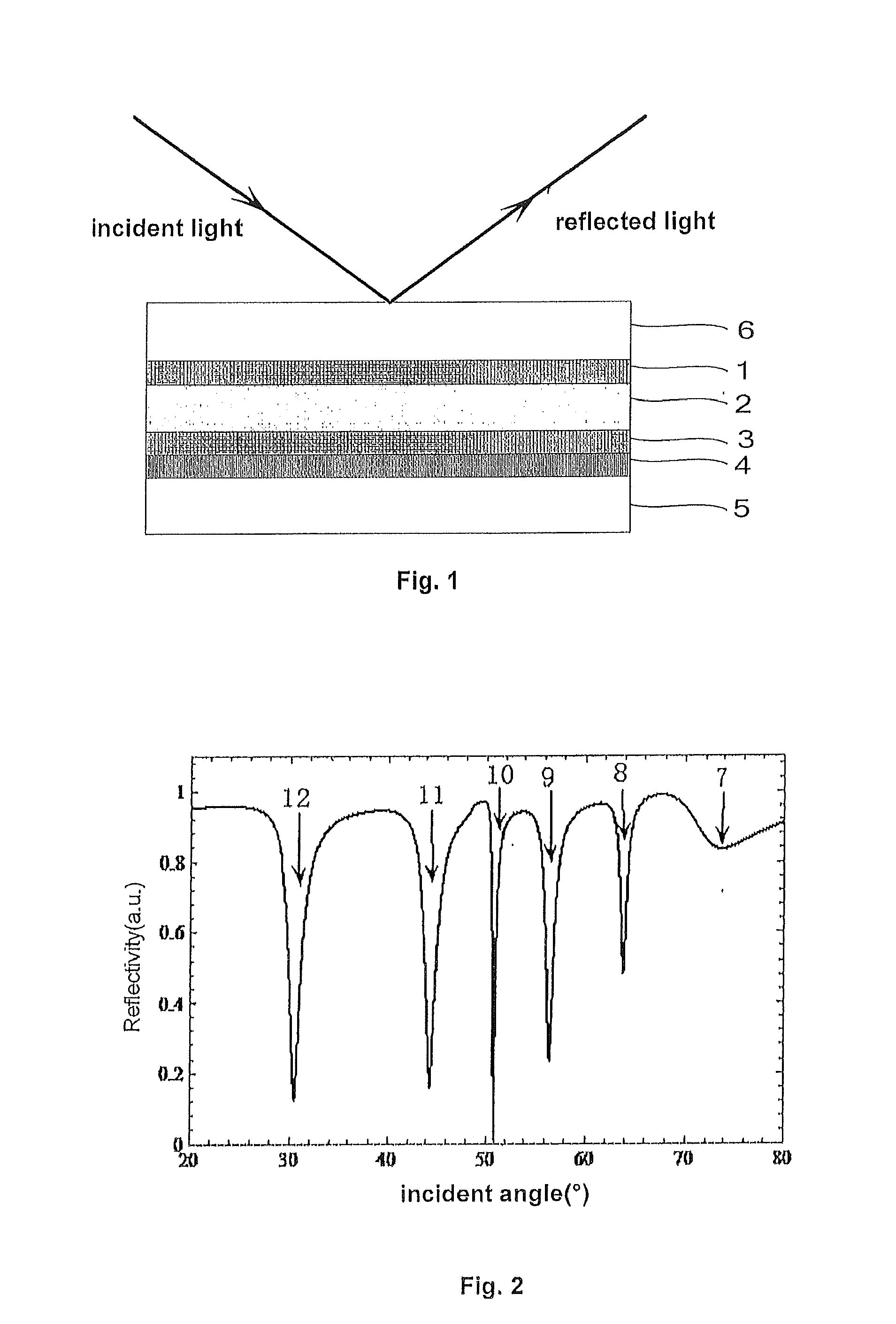
[0083]The WCSPR structure illustrated in FIG. 1 comprises a multilayer film structure. The SPR excited at the interface between the metal layer 3 and the detected layer 4 is affected by the waveguide modal property of the dielectric waveguide layer 2. Since the SPR can only be excited by a TM mode of the incident light, the reflection of the TM mode at the interface between the dielectric waveguide layer 2 and the metal layer 3 may be expressed as:

ri,k=kzlɛk-kzkɛlkzlɛk+kzkɛl(3)

[0084]where ri,k is the reflectivity of the light wave at the interface between the ith and kth layers, i,k=0, 1, 2 . . . , kzi=k0√...


PUM


Abstract

A sensor chip based on the WCSPR effect and an array thereof are disclosed. The sensor chip is a multilayer structure comprising a substrate, a dielectric waveguide layer (26) disposed on the substrate and a first metal layer (27) disposed on the dielectric waveguide layer (26), wherein parameters of physical properties of the dielectric waveguide layer (26) are tunable.

Description

FIELD OF THE INVENTION[0001]The present invention relates to the field of sensor and sensing technology, and more specifically to a Surface Plasmon Resonance (SPR) detection method with high resolution and fast response, a detection device and a detection array for implementing the method and the use thereof.BACKGROUND ART OF THE INVENTION[0002]Surface Plasmon (SP) is an oscillation mode resulted from the collective oscillation of charges on a metal surface propagating along a metal-dielectric interface. SP waves are found at the interface between two materials (generally metal and dielectric) with opposite-signed dielectric constants. The field intensity of this mode reaches the maximum at the interface, and decays exponentially in a direction normal to the interface on both sides of the surface. As a result, the modal field is restricted to the vicinity of the interface. The dispersion relation of the SP waves is expressed as:ksp=2πλ(ɛ1ɛ2ɛ1+ɛ2)1 / 2=ωc(ɛ1ɛ2ɛ1+ɛ2)1 / 2(1)where ksp is t...

Claims


Application Information

Patent Timeline
IPC IPC(8): G01J4/04H01L27/144H01L31/0232
CPCG01N21/553
Inventor ZHU, JINSONGXU, XINLONGFAN, JIANGFENGWANG, KUNWANG, CHENPISCOPIO, ANTHONY D.
Owner THE NAT CENT FOR NANOSCI & TECH NCNST OF CHINA
Learn More