Semiconductor light-emitting device and process for production thereof

Active Publication Date: 2011-03-03
KK TOSHIBA
View PDF7 Cites 21 Cited by
  • Summary
  • Abstract
  • Description
  • Claims
  • Application Information

AI Technical Summary

Benefits of technology

[0035]The light-emitting device of the present invention has a metal electrode covering the whole surface of the light-emitting part, and hence heat generated from inside of the device can be effectively dissipated via the metal electrode. Accordingly, even if much electric current flows in the device, the luminance intensity is not lowered. This means that the luminance intensity does not change or increases when the electric current increases. The metal electrode covering the whole light-emit

Problems solved by technology

However, enlarging the pad electrode is not effective in expanding the light-emitting part, and hence, practically a fine wire electrode is additionally put from the pad electrode along the semiconductor layer surface so that the light-emitting part can be expanded.
On the other hand, if the fine wire electrode is extended, it generally has a problem of making the electrode structure complicated.
A large reas

Method used


Image

  • Semiconductor light-emitting device and process for production thereof
  • Semiconductor light-emitting device and process for production thereof
  • Semiconductor light-emitting device and process for production thereof

Examples


Example

Example 1

[0126]In accordance with the aforementioned process, a semiconductor light-emitting device was produced. In Example 1, the device was made 300 μm square in size, which is the same as a conventional device, so that the device comprising a metal electrode provided with openings could be evaluated in properties comparatively with a conventional device.

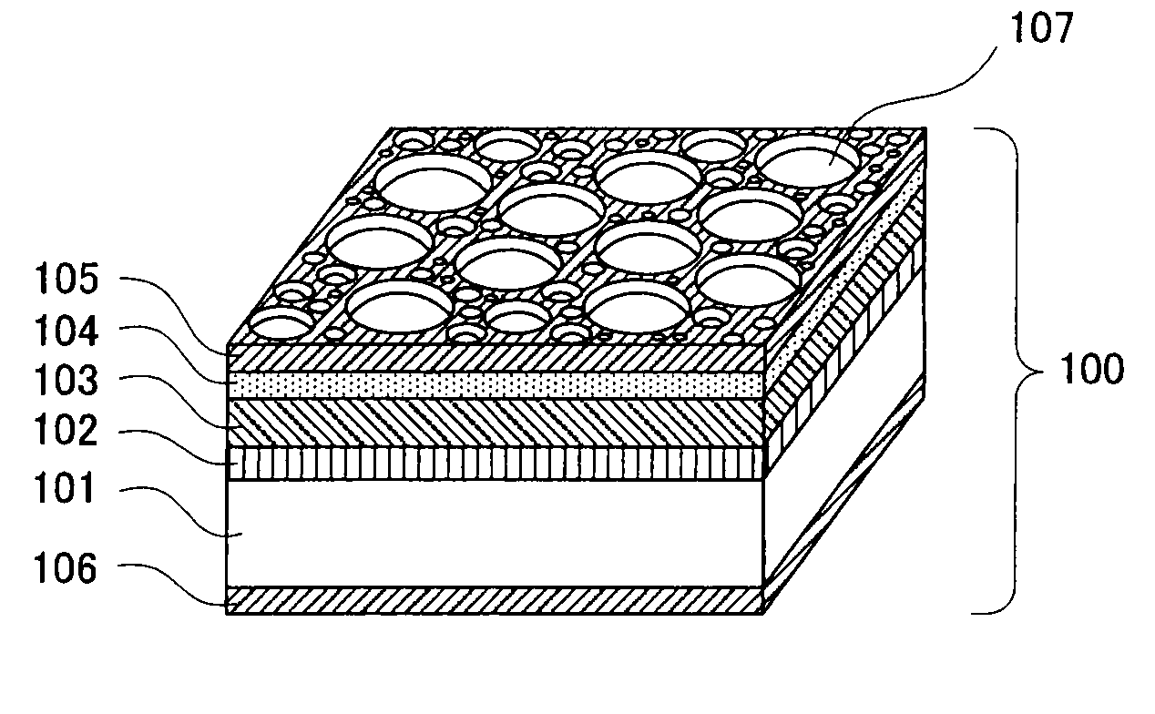
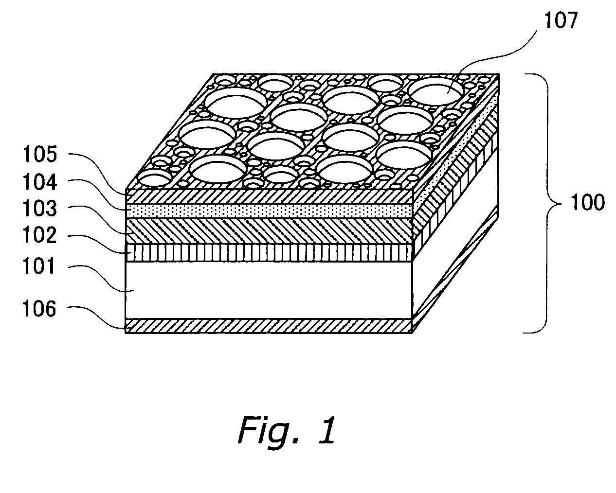
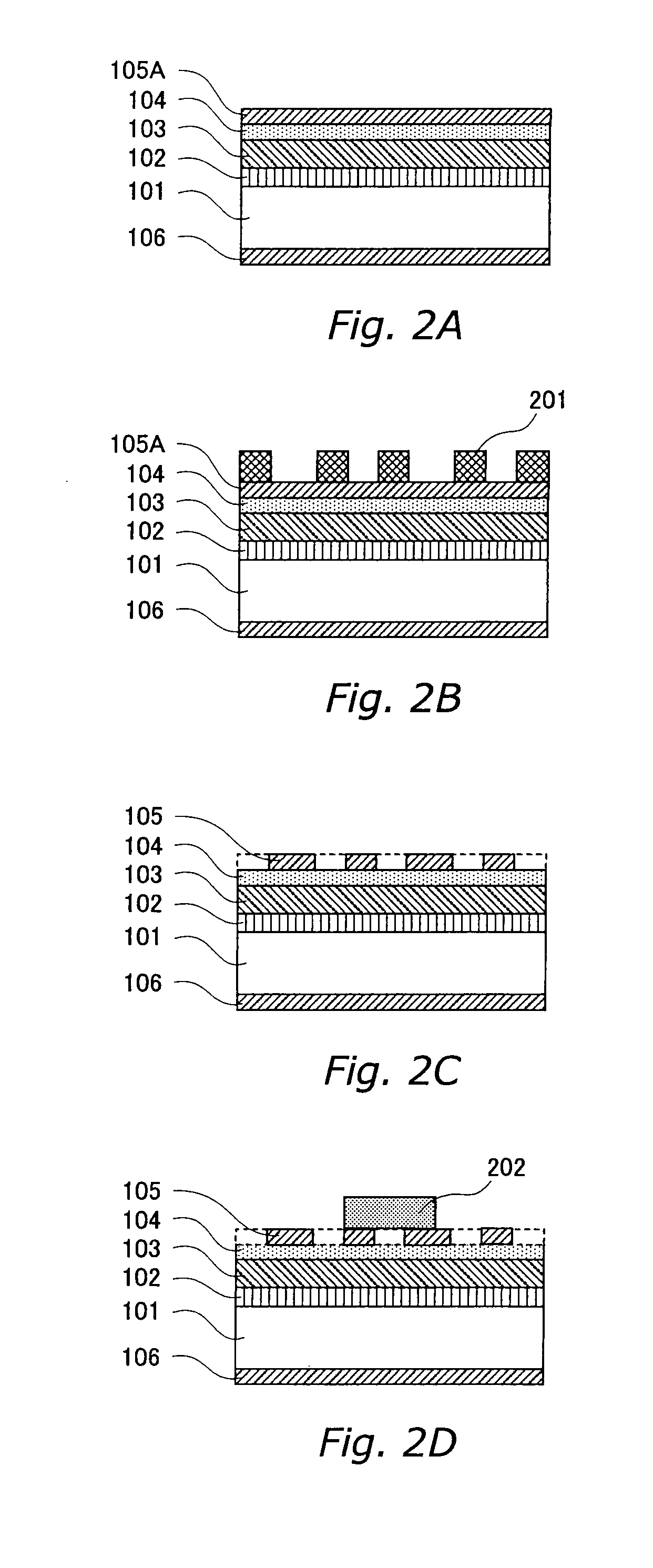
[0127]As shown in FIG. 2A, a hetero structure 102 including an n-type InAlP clad layer, an InGaP active layer and a p-type InAlP clad layer was formed on an n-GaAs substrate 101. Further, a current-spreading layer 103 of four-elemental p-type InGaAlP was epitaxially grown thereon. On the current-spreading layer thus formed, a p-type GaAs contact layer 104 (0.1 μm) was formed so as to ensure ohmic contact. On the opposite side of the substrate, an n-type counter electrode 106 was provided.

[0128]Subsequently, on the p-type GaAs contact layer, a metal thin layer 105A of Au (10 nm) / Au—Zn (3%) (30 nm) was formed by vapor deposition. T...

Example

Example 2

[0134]A semiconductor light-emitting device having the structure of n-GaAs / n-InAlP / InGaP / p-InAlP / p-InGaAlP / p-GaAs, which was similar to the device of Example 1, was prepared. The procedure of Example 1 was repeated to form a metal electrode layer provided with openings.

[0135]On the p-type GaAs layer, an Au (10 nm) / Au—Zn (3%) (30 nm) layer was formed by vapor deposition and thereafter annealed at 450° C. for 30 minutes in nitrogen gas atmosphere.

[0136]After that, the Au / Au—Zn layer was coated with an electron beam resist in the same manner as in Example 1, and treated by use of a pattern generator to form a hole pattern in which the diameter and interval of openings were 100 nm and 200 nm, respectively.

[0137]Subsequently, the Au / Au—Zn layer was etched by means of an ion-milling machine in the same manner as in Example 1, to form a metal electrode layer provided with openings. After the etching procedure, the resist was removed by oxygen ashing. Finally, a pad electrode was f...

Example

Example 3

[0140]A semiconductor light-emitting device having the structure of n-GaAs / n-InAlP / InGaP / p-InAlP / p-InGaAlP / p-GaAs, which was similar to the device of Example 1, was prepared. On the p-type GaAs layer 104, a metal thin layer 105A of Au (10 nm) / Au—Zn (3%) (30 nm) was formed by vapor deposition and thereafter annealed at 450° C. for 30 minutes in nitrogen gas atmosphere (FIG. 5A).

[0141]After that, the Au / Au—Zn layer was coated with an i-ray resist (THMR-iP3650 [trademark], manufactured by TOKYO OHKA KOGYO CO., LTD.) to form a resist layer of 1 μm thickness. The resist layer was treated by use of an i-ray stepper exposure system, to form a hole pattern in which the diameter and interval of openings were 500 nm and 1 μm, respectively (FIG. 5B).

[0142]Subsequently, the Au / Au—Zn layer was etched by means of an ion-milling machine in the same manner as in Example 1, to form a metal electrode layer 105 provided with openings. After the etching procedure, the i-ray resist was removed ...


PUM


Abstract

The present invention provides a semiconductor light-emitting device capable of keeping high luminance intensity even if electric power increases, and hence the device is suitable for lighting instruments such as lights and lamps. This semiconductor device comprises a metal electrode layer provided with openings, and is so large in size that the electrode layer has, for example, an area of 1 mm2 or more. The openings have a mean diameter of 10 nm to 2 μm, and they penetrate through the metal electrode layer. That metal electrode layer can be produced by use of self-assembling of block copolymer or by nano-imprinting techniques.

Description

CROSS-REFERENCE TO RELATED APPLICATION[0001]This application is based upon and claims the benefit of priority from the prior Japanese Patent Application No. 2009-199416, filed on Aug. 31, 2009; the entire contents of which are incorporated herein by reference.BACKGROUND OF THE INVENTION[0002]1. Field of the Invention[0003]This invention relates to a semiconductor light-emitting device comprising a metal electrode provided with openings. In detail, the present invention relates to a semiconductor light-emitting device improved in luminance properties.[0004]2. Background Art[0005]Recently, semiconductor light-emitting devices have been studied for application to displays or to lighting instruments such as lights and lamps. The semiconductor light-emitting device generally comprises electrodes and a semiconductor layer placed between them, and emits luminescence when electric current flows between the electrodes. Normally, the device has a pad electrode in ohmic contact with the semico...

Claims


Application Information

Patent Timeline
IPC IPC(8): H01L33/40
CPCH01L33/38H01L2933/0083H01L33/40
Inventor FUJIMOTO, AKIRAKITAGAWA, RYOTAASAKAWA, KOJI
Owner KK TOSHIBA
Why Eureka
Try Eureka