Organic electroluminescent element, method for manufacturing the organic electroluminescent element, and light emitting display device

a technology of organic electroluminescent elements and electroluminescent elements, which is applied in the direction of solid-state devices, semiconductor devices, thermoelectric devices, etc., can solve the problems of lowering the current density, ionizing electrons, and lowering luminescence characteristics, so as to facilitate the injection of charges and reduce damage to the organic layer

Inactive Publication Date: 2011-03-31
DAI NIPPON PRINTING CO LTD
View PDF5 Cites 10 Cited by
  • Summary
  • Abstract
  • Description
  • Claims
  • Application Information

AI Technical Summary

Benefits of technology

[0014]Accordingly, an object of the present invention is to provide an organic electroluminescent element having an element structure that can reduce damage to an organic layer during electrode formation and can facilitate the injection of charges from the electrode into the organic layer, and a method for manufacturing the organic electroluminescent element. Another object of the present invention is to provide a light emitting display device comprising the organic electroluminescent element.

Problems solved by technology

Since, however, the transparent electroconductive film formed of ITO or the like is generally formed by sputtering, in the organic EL element having the above construction, the formation of the transparent electroconductive film on the electron injection layer poses a problem of causing lowered luminescence characteristics as a result of damage to the organic luminescent layer or the electron injection layer due to impact of sputtered particles or argon ions (Ar+), ionized electrons or the like during sputtering, for example, lowered current density, lowered luminescence efficiency, and the occurrence of leak current.
Further, the use of plasma in the formation of the transparent electroconductive film poses a problem of causing lowered luminescence characteristics as a result of undergoing the same damage as described above due to exposure of the organic luminescent layer or the electron injection layer to a plasma atmosphere.
Furthermore, in the formation of the transparent electroconductive film, problems occur including a problem of causing lowered electron injection properties as a result of oxidation of a highly reactive metal such as aluminum (Al) constituting the electron injection layer by oxygen in the atmosphere or oxygen released from a target, for example, lowered current density characteristics, lowered luminescence efficiency, and increased dark spots.
In particular, unsatisfactory electron transport properties and electron injection properties pose a problem of causing a lowering in current-voltage characteristics due to an increase in electric resistance as the whole element and, at the same time, causing a lowering in luminescence characteristics due to loss of balance between holes and electrons injected into the organic luminescent layer.
Furthermore, since the semi-transparent cathode layer is formed of a highly reactive material such as an alkali metal as a simple substance, in the region where the semi-transparent cathode layer is in contact with the transparent electroconductive protective layer, the transparent electroconductive protective layer sometimes undergoes damage such as oxidation in the formation of the transparent electroconductive protective layer.

Method used


Image

  • Organic electroluminescent element, method for manufacturing the organic electroluminescent element, and light emitting display device
  • Organic electroluminescent element, method for manufacturing the organic electroluminescent element, and light emitting display device
  • Organic electroluminescent element, method for manufacturing the organic electroluminescent element, and light emitting display device

Examples


example 1

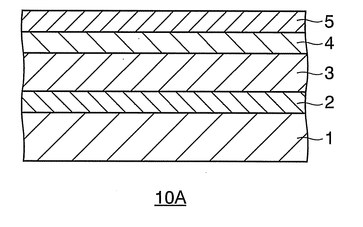
[0146]An ITO substrate was first provided. The ITO substrate had a 150 nm-thick line-patterned anode 2 of ITO (line width: 2 mm) provided on a transparent base material 1 formed of a glass substrate. TBADN represented by chemical formula 5 above and MoO3 as an oxidizing dopant were codeposited on the ITO substrate at a deposition rate of 1.5 angstroms / sec under a degree of vacuum of 10-5 Pa so that the weight ratio of TBADN to MoO3 was 67:33, thereby forming a 10 nm-thick hole injection layer.

[0147]TBADN represented by chemical formula 5 as described above was then vacuum-deposited on the hole injection layer at a deposition rate of 1.0 angstrom / sec under a degree of vacuum of 10-5 Pa to form a 10 nm-thick hole transport layer. The laminate composed of the hole injection layer and the hole transport layer can be said to be a hole injection / transport layer 3a having an oxidizing dopant-mixed region (hole injection layer) on the anode side.

[0148]TCTA represented by chemical formula 6 ...

example 2

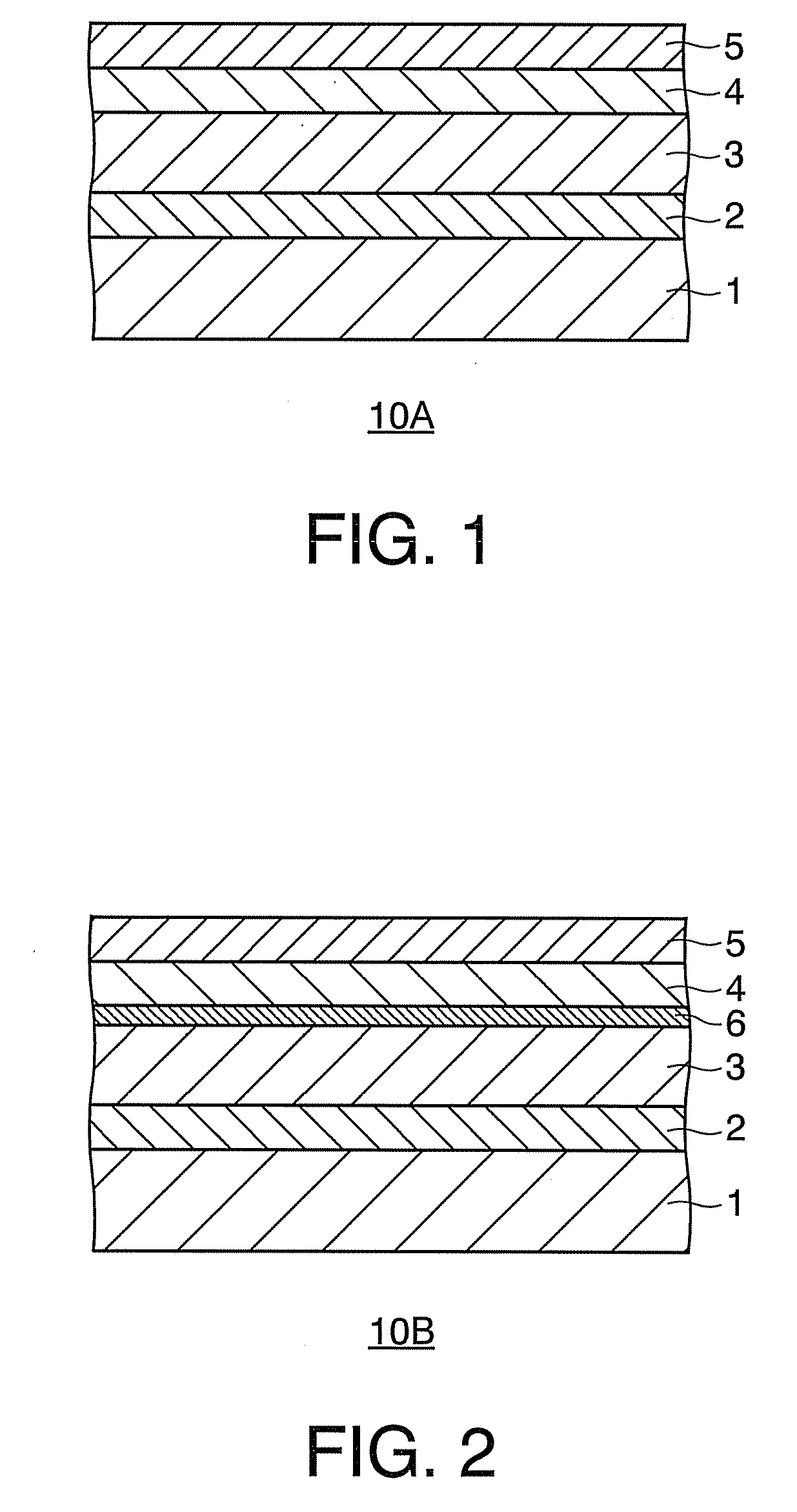
[0158]An organic EL element of Example 2 was prepared in the same manner as in Example 1, except that, in the organic EL element of Example 1, an electroconductive layer 6 of aluminum (thickness 2 nm) was formed between the electron injection / transport layer 3c and the transparent protective layer 4 at a deposition rate of 0.5 angstrom / sec under a degree of vacuum of 10-5 Pa. The organic EL element of Example 2 was observed under a scanning electron microscope. As a result, the formed 2 nm-thick Al was in an sea-island form.

example 3

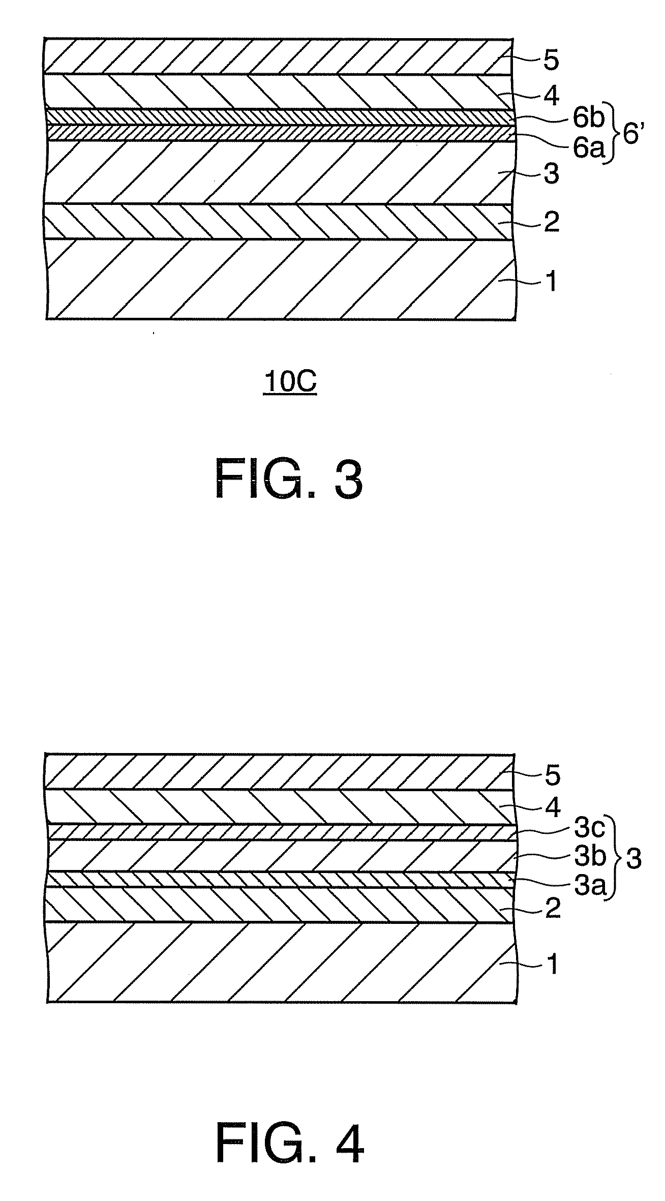
[0162]An organic EL element of Example 3 was prepared in the same manner as in Example 1, except that, in the organic EL element of Example 1, an electroconductive layer 6′ was provided between the electron injection / transport layer 3c and the transparent protective layer 4 by forming a first electroconductive layer 6a of Al (thickness 2 nm) from the electron injection / transport layer 3c side at a deposition rate of 0.5 angstrom / sec under a degree of vacuum of 10-5 Pa and further forming a second electroconductive layer 6b of MgAg (thickness 5 nm) on the first electroconductive layer 6a at a deposition rate of 1 angstrom / sec under a degree of vacuum of 10-5 Pa.


PUM


Abstract

Disclosed is an organic electroluminescent element having an element structure that can reduce damage to an organic layer during electrode formation and can facilitate the injection of charges from the electrode into the organic layer. The organic electroluminescent element includes an anode, a cathode, and an organic layer held between the anode and the cathode. The organic layer contains a luminescent material. The organic electroluminescent element further includes a transparent protective layer provided between the anode or the cathode and the organic layer. The transparent protective layer contains a bipolar charge transport organic compound and an electron-accepting compound. The transparent protective layer is formed in a period between after the formation of the organic layer and before the formation of the anode or the cathode on the organic layer.

Description

BACKGROUND OF THE INVENTION[0001]1. Field of Invention[0002]The present invention relates to an organic electroluminescent element, a method for manufacturing the organic electroluminescent element, and a light emitting display device using the organic electroluminescent element. More specifically, the present invention relates to an organic electroluminescent element having an element structure that can reduce damage to an organic layer during electrode formation and can facilitate the injection of charges from the electrode into the organic layer, and a method for manufacturing the organic electroluminescent element and a light emitting display device using the organic luminescent element.[0003]2. Background Art[0004]An organic electroluminescent element, which comprises a luminescent material-containing organic luminescent layer held between a pair of electrodes and emits light by applying voltage across both the electrodes (hereinafter sometimes referred to as an organic EL elem...

Claims


Application Information

Patent Timeline
Patent Type & Authority Applications(United States)
IPC IPC(8): H01L51/50H01L33/42
CPCH01L51/5221H01L51/5048H10K50/14H10K50/82
Inventor NAKAJIMA, HIROYOSHISHIMOGAWARA, MASAYAIIZUMI, YASUHIRO
Owner DAI NIPPON PRINTING CO LTD
Why Eureka
Try Eureka