Method for controlling threshold voltage of semiconductor element

Active Publication Date: 2011-03-31
CANON KK
View PDF16 Cites 63 Cited by
  • Summary
  • Abstract
  • Description
  • Claims
  • Application Information

AI Technical Summary

Benefits of technology

[0044]In addition, in a plurality of elements included in a semiconductor device, the fluctuation of threshold voltage between elements can be suppressed.
[0045]Furthermore, in a

Problems solved by technology

However, in any of the above-described documents concerning oxide TFTs, methods for compensating or suppressing change in the threshold voltage due to the causes, and methods for relatively reducing the effects of change in the threshold voltage are not clarified.
However, such a correcting circuit is a complicated circuit containing semiconductor element, and the separate provision of the correcting circuit enlarges and complicates the entire circuit and expands fabricating costs.
Also when change in the threshold voltage is extremely large

Method used


Image

  • Method for controlling threshold voltage of semiconductor element
  • Method for controlling threshold voltage of semiconductor element
  • Method for controlling threshold voltage of semiconductor element

Examples


embodiments

[0167]Although the embodiments of the present invention will be described hereunder, the present invention is not limited to the following embodiments.

first embodiment

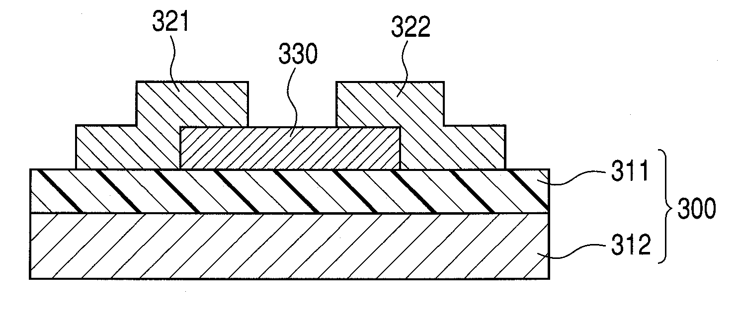
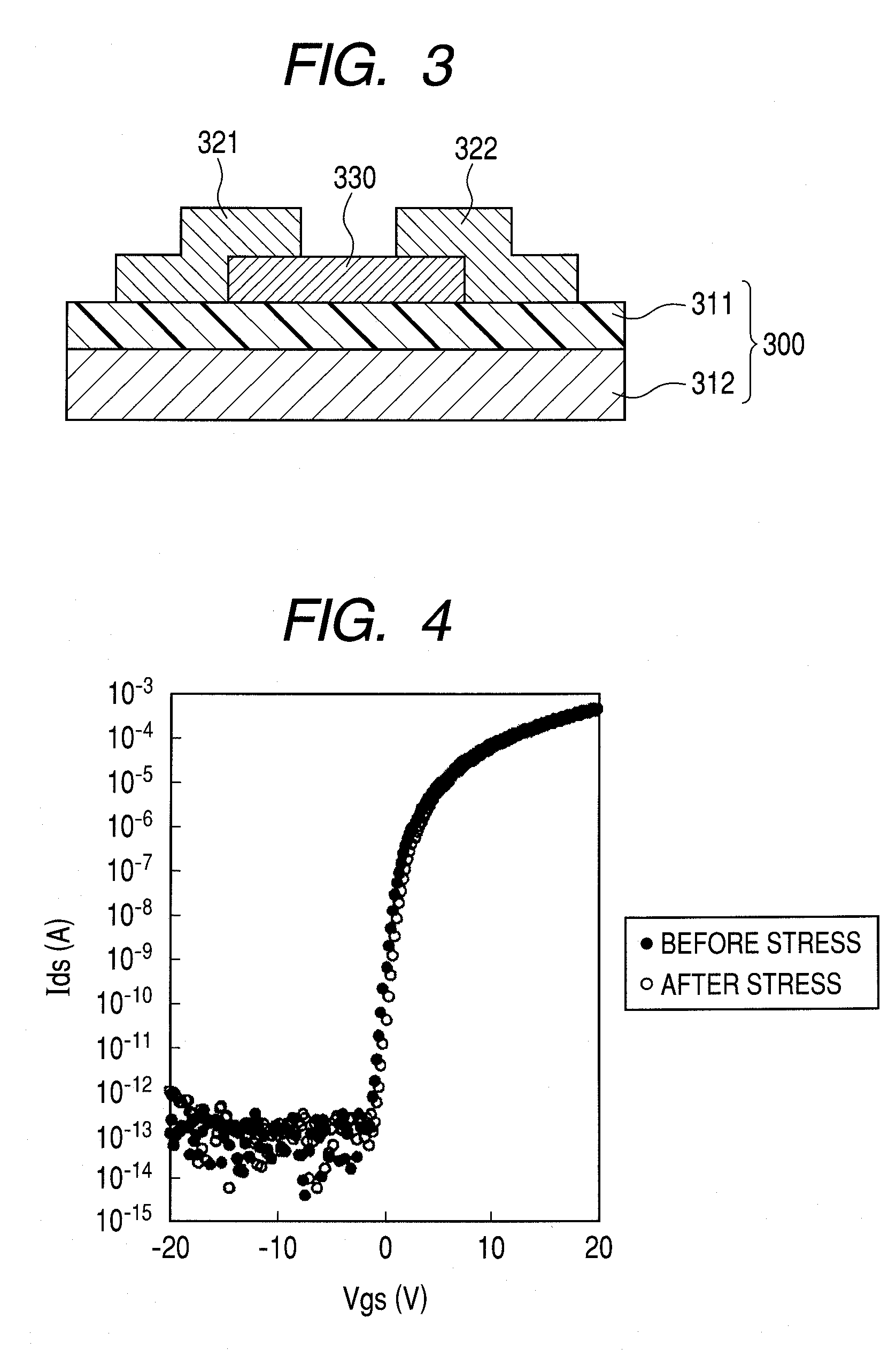
[0168]In the first embodiment, an amorphous GZO-TFT of a reverse stagger type was fabricated on a glass substrate through the following procedures. The sectional view of the TFT is shown in FIG. 9.

[0169]First, a glass substrate (Corning 1737) was cleaned, and was used as a substrate. On the substrate, a titanium-gold laminated film having a total thickness of 50 nm was laminated by an electron beam vapor deposition method, and the laminated film was patterned by a lift-off method to obtain the gate electrode 312. Thereon, a SiO2 film having a thickness of 200 nm was laminated by an RF magnetron sputtering method (film forming gas: Ar, film forming pressure: 0.1 Pa, and applied power: 400 W) using SiO2 as a target. This was patterned by etching to obtain the gate insulating layer 311. Thereon, an amorphous IGZO having a thickness of 20 nm was laminated by an RF magnetron sputtering method (film forming gas: O2 (5% by volume)+Ar (95% by volume), film forming pressure: 0.5 Pa, and appl...

second embodiment

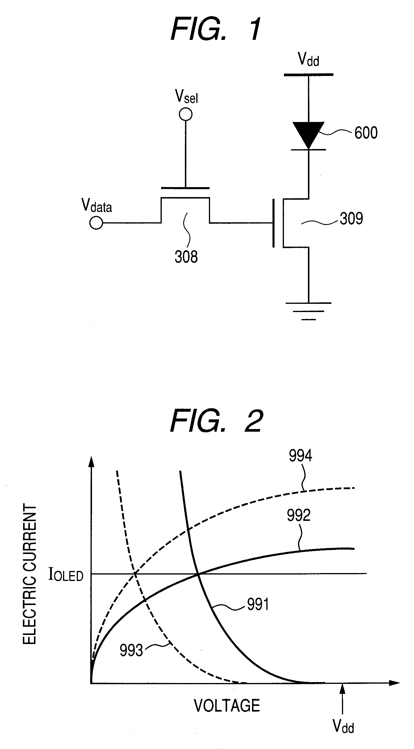
[0176]In the second embodiment, the system wherein external circuits are added to the semiconductor device was established. The connections are schematically shown in FIG. 13.

[0177]A TFT driving circuit is connected to the TFT, and contains the power source and the like for making the TFT carry out the intended operations (such as the driving of loads (not shown) connected to the TFT). The Vth measuring circuit can be connected to the TFT optionally switching to the TFT driving circuit, and measures the Vth of the TFT and outputs the Vth to the light emitting diode control circuit. In the second embodiment, the Vth measuring circuit is made to have a variable voltage source and an electric current measuring device, and has a configuration for measuring the transfer characteristics of the TFT to calculate Vth and output the Vth to the light emitting diode control circuit. The memory stores the lookup table for specifying the electric current to be applied to the light emitting diode ...


PUM


Abstract

A method for controlling the threshold voltage of a semiconductor element having at least a semiconductor as a component is characterized in including a process to measure one of a threshold voltage and a characteristic value serving as an index for the threshold voltage; a process to determine one of the irradiation intensity, irradiation time, and wavelength of the light for irradiating the semiconductor based on one of the measured threshold voltage and the measured characteristic value serving as the index for the threshold voltage; and a process to irradiate light whose one of the irradiation intensity, irradiation time, and wavelength has been determined onto the semiconductor; wherein the light irradiating the semiconductor is a light having a longer wavelength than the wavelength of the absorption edge of the semiconductor, and the threshold voltage is changed by the irradiation of the light.

Description

TECHNICAL FIELD[0001]The present invention relates to a method for controlling the threshold voltage of a semiconductor element using semiconductors.BACKGROUND ART[0002]A TFT back plane is a device wherein a plurality of thin film transistors (TFT) is arrayed on a substrate. Presently, an active matrix liquid crystal display and an active matrix organic electroluminescent display (organic EL display, organic light emitting diode display) using the TFT back plane are actively studied and developed. As the TFT, a hydrogenated amorphous silicon (a-Si:H) TFT and a low-temperature polycrystalline silicon (LTPS) TFT have been used.[0003]In such a TFT back plane, the improvement of threshold voltage stability and the improvement of in-plane uniformity are critical issues. For threshold voltage stability, the suppression of change in the threshold voltage of the TFT caused by various reasons (change with time, electrical stress, and thermal stress) is a critical issue. On the other hand, fo...

Claims


Application Information

Patent Timeline
IPC IPC(8): H01L21/66
CPCH01L29/66969H01L29/7869
Inventor OFUJI, MASATOTAKAI, YASUYOSHIKAWASAKI, TAKEHIKOKANEKO, NORIOHAYASHI, RYO
Owner CANON KK
Why Eureka
Try Eureka