

Semiconductor device and method for manufacturing the same
a semiconductor and semiconductor technology, applied in the field of semiconductor devices, can solve problems such as deviation from the stoichiometric composition of oxide semiconductors, and achieve the effect of stable electric characteristics
- Summary
- Abstract
- Description
- Claims
- Application Information
AI Technical Summary
Benefits of technology
Problems solved by technology
Method used
Image

Examples
embodiment 1
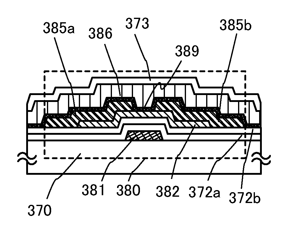
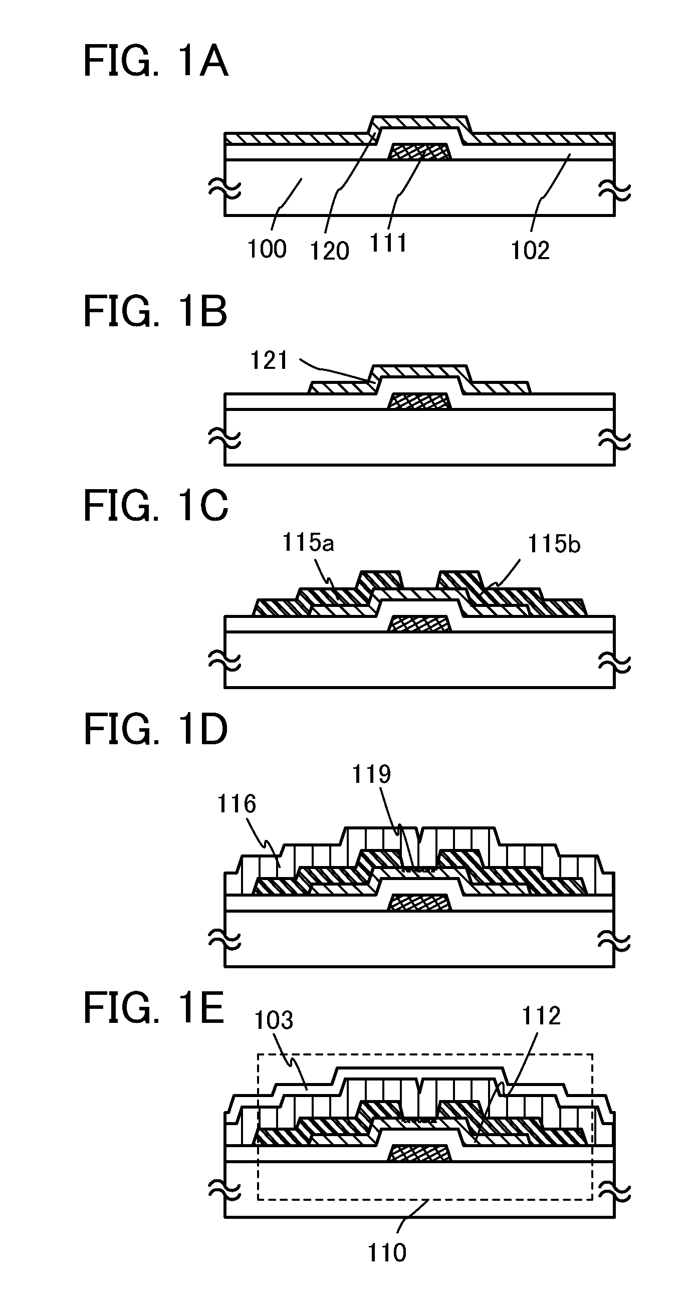
[0059]In this embodiment, an embodiment of a semiconductor device and a manufacturing method thereof will be described with reference to FIGS. 1A to 1E. The semiconductor device described in this embodiment is a thin film transistor.
[0060]FIGS. 1A to 1E illustrate an example of a cross-sectional structure of a semiconductor device. A thin film transistor 110 illustrated in FIGS. 1A to 1E has one type of a bottom-gate structure and is also referred to as an inverted staggered thin film transistor.
[0061]The thin film transistor 110 illustrated in FIGS. 1A to 1E includes, over a substrate 100 having an insulating surface, a gate electrode layer 111, a gate insulating layer 102, an oxide semiconductor layer 112, an oxygen-excess mixed region 119, a source electrode layer 115a, and a drain electrode layer 115b. In addition, an insulating layer 116 having defects which covers the thin film transistor 110 and overlaps with the oxide semiconductor layer 112 with the oxygen-excess mixed regi...
embodiment 2
[0158]In this embodiment, another example of a thin film transistor which can be applied to a semiconductor device disclosed in this specification will be described. The same portion as or a portion having a function similar to those in the above embodiment can be formed in a manner similar to that described in the above embodiment, and also the steps similar to those in the above embodiment can be performed in a manner similar to that described in the above embodiment, and repetitive description is omitted. In addition, detailed description of the same portions is not repeated.
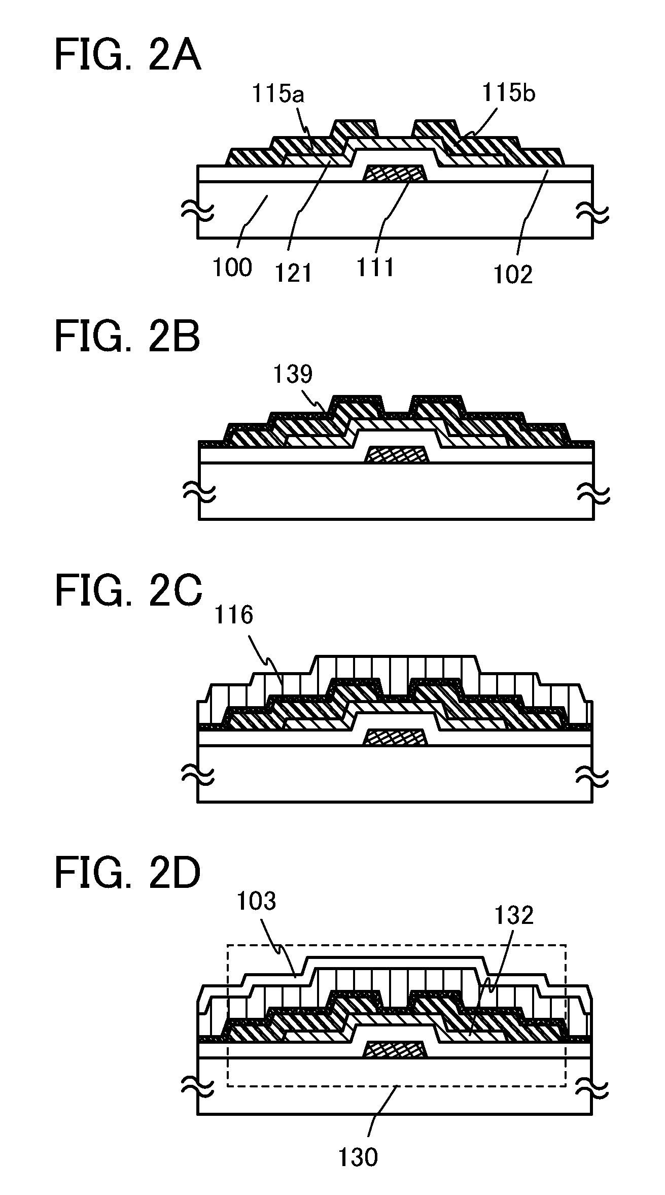
[0159]FIGS. 2A to 2D illustrate an example of a cross-sectional structure of a semiconductor device. A thin film transistor 130 illustrated in FIGS. 2A to 2D has one type of a bottom-gate structure and is also referred to as an inverted staggered thin film transistor.
[0160]The thin film transistor 130 illustrated in FIGS. 2A to 2D includes, over the substrate 100 having an insulating surface, the gate electro...
embodiment 3
[0191]In this embodiment, another example of a thin film transistor which can be applied to a semiconductor device disclosed in this specification will be described.
[0192]A semiconductor device and a manufacturing method thereof in this embodiment will be described with reference to FIGS. 3A to 3E.
[0193]FIGS. 3A to 3E illustrate an example of a cross-sectional structure of a semiconductor device. A thin film transistor 160 illustrated in FIGS. 3A to 3E has one type of a bottom-gate structure called a channel-protective structure (also referred to as a channel-stop structure) and is also referred to as an inverted staggered thin film transistor.
[0194]Although the thin film transistor 160 is described as a single-gate thin film transistor, a multi-gate thin film transistor including a plurality of channel formation regions can be formed if needed.
[0195]Hereinafter, a process for manufacturing the thin film transistor 160 over the substrate 150 will be described with reference to FIGS....
PUM
 Abstract
Description
Claims
Application Information