Nonvolatile latch circuit and logic circuit, and semiconductor device using the same

a logic circuit and latch circuit technology, applied in pulse generators, pulse techniques, instruments, etc., can solve the problems of large variation influence, high-accuracy reading circuits, and large number of rewrites of nonvolatile latch circuits using ferroelectric elements, etc., to achieve wide operating temperature range, low cost, and low cost

Active Publication Date: 2011-05-26
SEMICON ENERGY LAB CO LTD
View PDF32 Cites 211 Cited by
  • Summary
  • Abstract
  • Description
  • Claims
  • Application Information

AI Technical Summary

Benefits of technology

[0020]According to an embodiment of the present invention, with the use of a transistor using an oxide semiconductor as a semiconductor material for forming a channel formation region, which serves as a switching element of a data holding portion, a nonvolatile latch circuit which has a wide operating temperature range and operates stably even at a high temperature and in which a logical state of storing data is not erased even after the power is turned off, or a latch circuit provided with a data holding portion where a refresh period is sufficiently long can be realized. Since data writing is performed by switching of the transistor, the number of rewrites is not substantially limited. In addition, the writing voltage is almost equivalent to the threshold voltage of the transistor; thus, the t

Problems solved by technology

However, a nonvolatile latch circuit using a ferroelectric element has problems in terms of reliability of the number of rewrites and reduction in voltage.
However,

Method used


Image

  • Nonvolatile latch circuit and logic circuit, and semiconductor device using the same
  • Nonvolatile latch circuit and logic circuit, and semiconductor device using the same
  • Nonvolatile latch circuit and logic circuit, and semiconductor device using the same

Examples


embodiment 1

[0050]In this embodiment, an example of a configuration and an operation of a nonvolatile latch circuit which is an embodiment of the invention disclosed herein, a method for manufacturing an element included in the nonvolatile latch circuit, and the like will be described with reference to FIGS. 1A and 1B, FIGS. 2A and 2B, FIGS. 3A and 3B, FIGS. 4A to 4H, FIGS. 5A to 5G, FIGS. 6A to 6D, FIG. 7, FIG. 8, FIGS. 9A and 9B, FIG. 10, FIG. 11, FIG. 12, FIG. 13, FIG. 14, FIG. 15, FIG. 16, and FIG. 17.

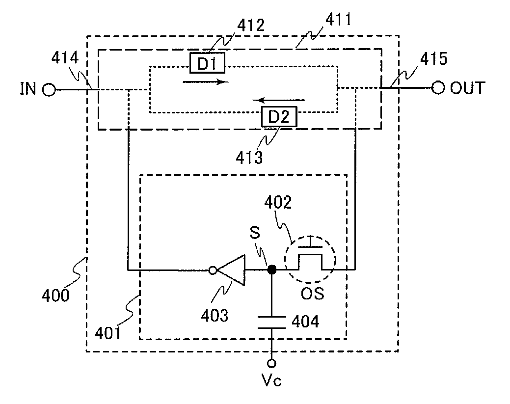
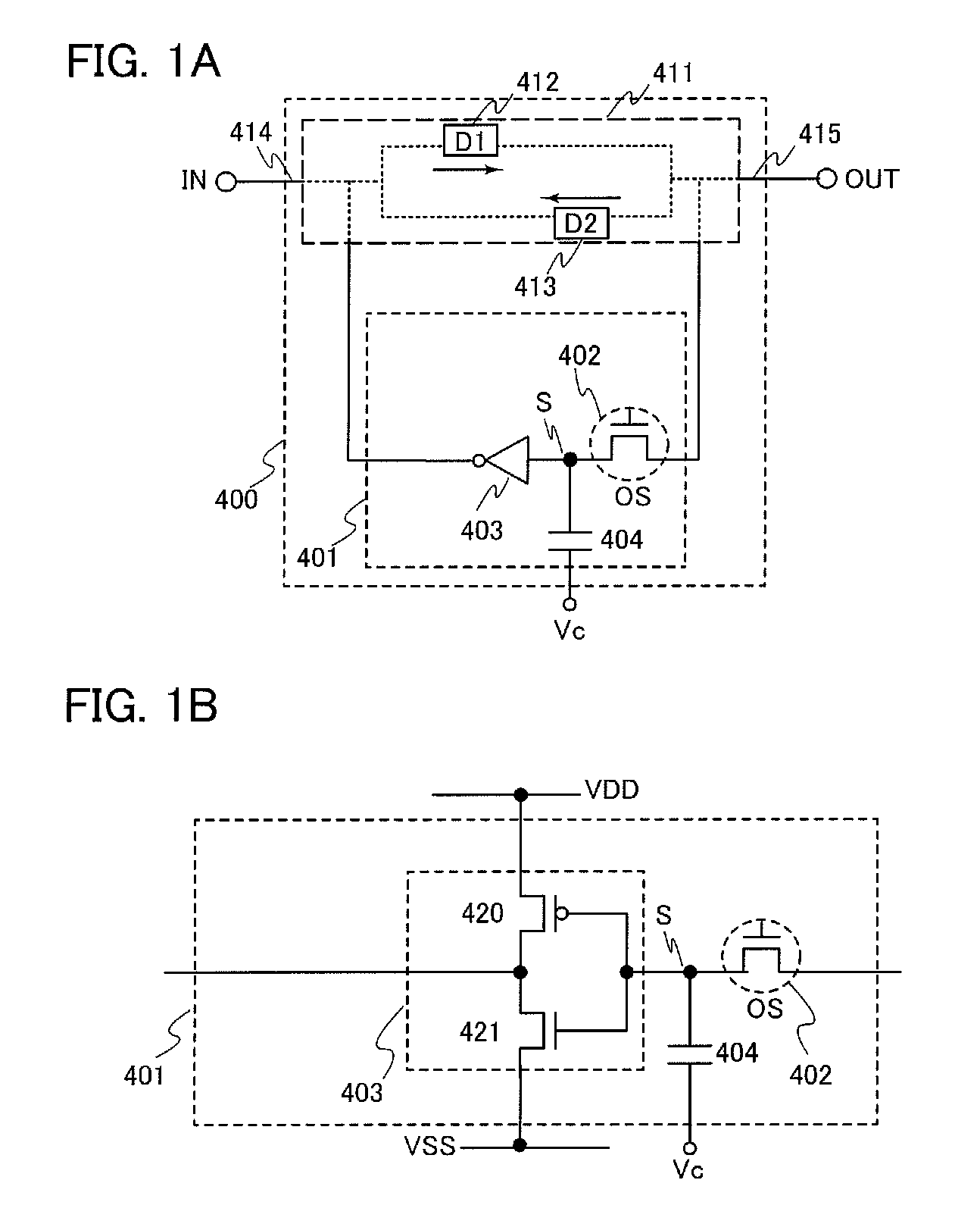
[0051]FIG. 1A illustrates a configuration of a nonvolatile latch circuit 400 including a latch portion 411 and a data holding portion 401 for holding data of the latch portion. FIG. 1B illustrates a configuration of the data holding portion 401.

[0052]The nonvolatile latch circuit 400 in FIG. 1A includes the latch portion 411 having a loop structure and the data holding portion 401 for holding data of the latch portion. In the latch portion 411 having a loop structure, an output of a first elem...

embodiment 2

[0199]In this embodiment, another example of a configuration of the nonvolatile latch circuit which is an embodiment of the invention disclosed herein, which is different from the example in FIGS. 1A and 1B, will be described with reference to FIGS. 18A and 18B. FIG. 18A illustrates a configuration of a nonvolatile latch circuit 400 including the latch portion 411 and a data holding portion 401 for holding data of the latch portion. FIG. 18B illustrates a configuration of the data holding portion 401.

[0200]FIGS. 18A and 18B illustrate an example in which the configuration of the data holding portion 401 is different from that in FIGS. 1A and 1B. Specifically, a capacitor (the capacitor 404 in FIGS. 1A and 1B) of the data holding portion 401 is not provided in this example. The other configurations are the same as that of FIGS. 1A and 1B; therefore, description thereof is omitted. The structure of the transistor 402 is similar to that in Embodiment 1.

[0201]In the data holding portion...

embodiment 3

[0210]In this embodiment, an example of a configuration and an operation of the nonvolatile latch circuit which is an embodiment of the invention disclosed herein will be described with reference to FIGS. 19A and 19B and FIGS. 1A and 1B.

[0211]FIG. 19A illustrates a configuration of the nonvolatile latch circuit 400 including the latch portion 411 and the data holding portion 401 for holding data of the latch portion. FIG. 19B illustrates an example of a timing chart of the nonvolatile latch circuit 400.

[0212]FIG. 19A is an example in which the configuration of the latch portion 411 in FIG. 1A is specifically illustrated. FIG. 19A is an example of the configuration of the latch portion 411 in FIG. 1A, where an inverter is used for each of the first element and the second element. The structure of the transistor 402 is similar to that in Embodiment 1.

[0213]The latch portion 411 includes an inverter 412 and an inverter 413. The latch portion 411 has a loop structure in which an output ...


PUM


Abstract

To provide a novel nonvolatile latch circuit and a semiconductor device using the nonvolatile latch circuit, a nonvolatile latch circuit includes a latch portion having a loop structure where an output of a first element is electrically connected to an input of a second element, and an output of the second element is electrically connected to an input of the first element; and a data holding portion for holding data of the latch portion. In the data holding portion, a transistor using an oxide semiconductor as a semiconductor material for forming a channel formation region is used as a switching element. In addition, an inverter electrically connected to a source electrode or a drain electrode of the transistor is included. With the transistor, data held in the latch portion can be written into a gate capacitor of the inverter or a capacitor which is separately provided.

Description

TECHNICAL FIELD[0001]The invention disclosed herein relates to a nonvolatile logic circuit in which the logical state of storing data is not erased even after the power is turned off, and a semiconductor device using the nonvolatile logic circuit. In particular, the invention disclosed herein relates to a nonvolatile latch circuit and a semiconductor device using the nonvolatile latch circuit.BACKGROUND ART[0002]An integrated circuit has been proposed in which nonvolatile logic is integrated, where a feature of “nonvolatile” with which data is not erased even when the power is turned off is applied to a logic circuit. For example, a nonvolatile latch circuit using a ferroelectric element has been proposed as nonvolatile logic (see Patent Document 1).REFERENCEPatent Document[0003][Patent Document 1] PCT International Publication No. 2003 / 044953DISCLOSURE OF INVENTION[0004]However, a nonvolatile latch circuit using a ferroelectric element has problems in terms of reliability of the nu...

Claims


Application Information

Patent Timeline
IPC IPC(8): H03K3/00
CPCG11C7/04H03K3/356G11C16/045G11C2211/4016H01L21/02554H01L21/02565H01L21/02631H01L21/28202H01L21/28211H01L27/105H01L27/1203H01L27/1225H01L29/6659H03K3/0375H03K3/356121H03K3/356173H03K3/286G11C14/0063G11C16/06H03K3/356104
Inventor KATO, KIYOSHIKOYAMA, JUN
Owner SEMICON ENERGY LAB CO LTD
Why Eureka
Try Eureka