

Method for manufacturing stacked film and solar cell
a technology of solar cells and stacked films, which is applied in the field of manufacturing stacked films, can solve the problems of adversely affecting electrical productivity, deteriorating electrical operation characteristics of resulting devices, etc., and achieve the effect of improving electrical operation characteristics of solar cells
- Summary
- Abstract
- Description
- Claims
- Application Information
AI Technical Summary
Benefits of technology
Problems solved by technology
Method used
Image

Examples
example 1
Manufacture of a Solar Cell
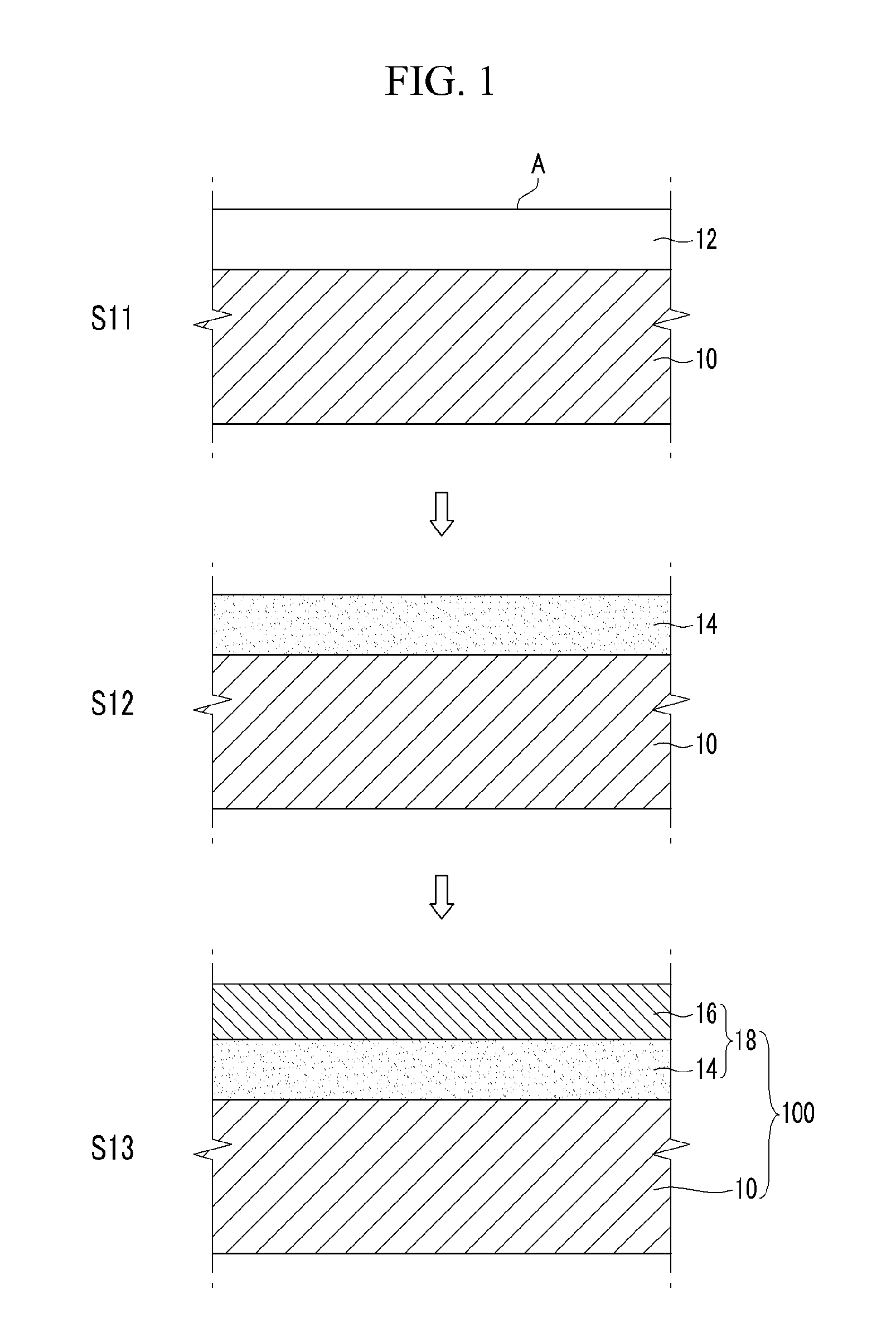
[0093]In the present example according to an exemplary embodiment, POCl3 is diffused into a pyramidally surface textured silicon wafer to dope the wafer with an n-type impurity
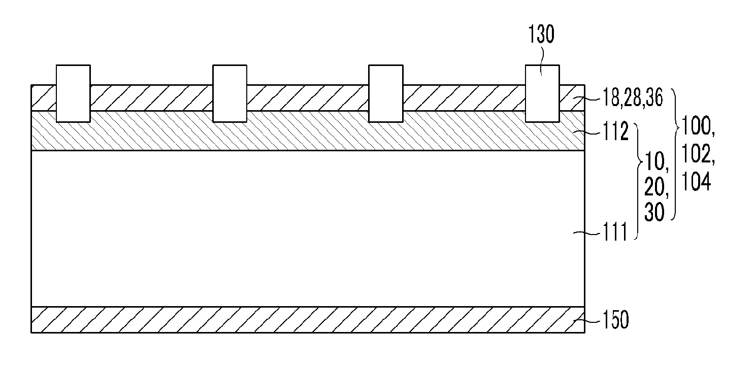
[0094]A gas containing oxygen gas / hydrogen gas (O2 / H2, 10 / 1 volume ratio) is flowed at a temperature of about 900° C. and under pressure of about 0.33 Torr, and reacted for about 7.5 hours to form an oxide layer. Then, the oxide layer is heat treated 1-5 times at about 400° C. while supplying a reaction gas containing about 3 volume % of hydrogen. A nitride layer (anti-reflection coating) is formed on the oxide layer to form a stacked film. A silver electrode (front electrode) is formed on the surface of the stacked film, and an aluminum electrode (rear electrode) is formed on the other surface of the stacked film to prepare an exemplary embodiment of a solar cell.
example 2
Manufacture of Solar Cell
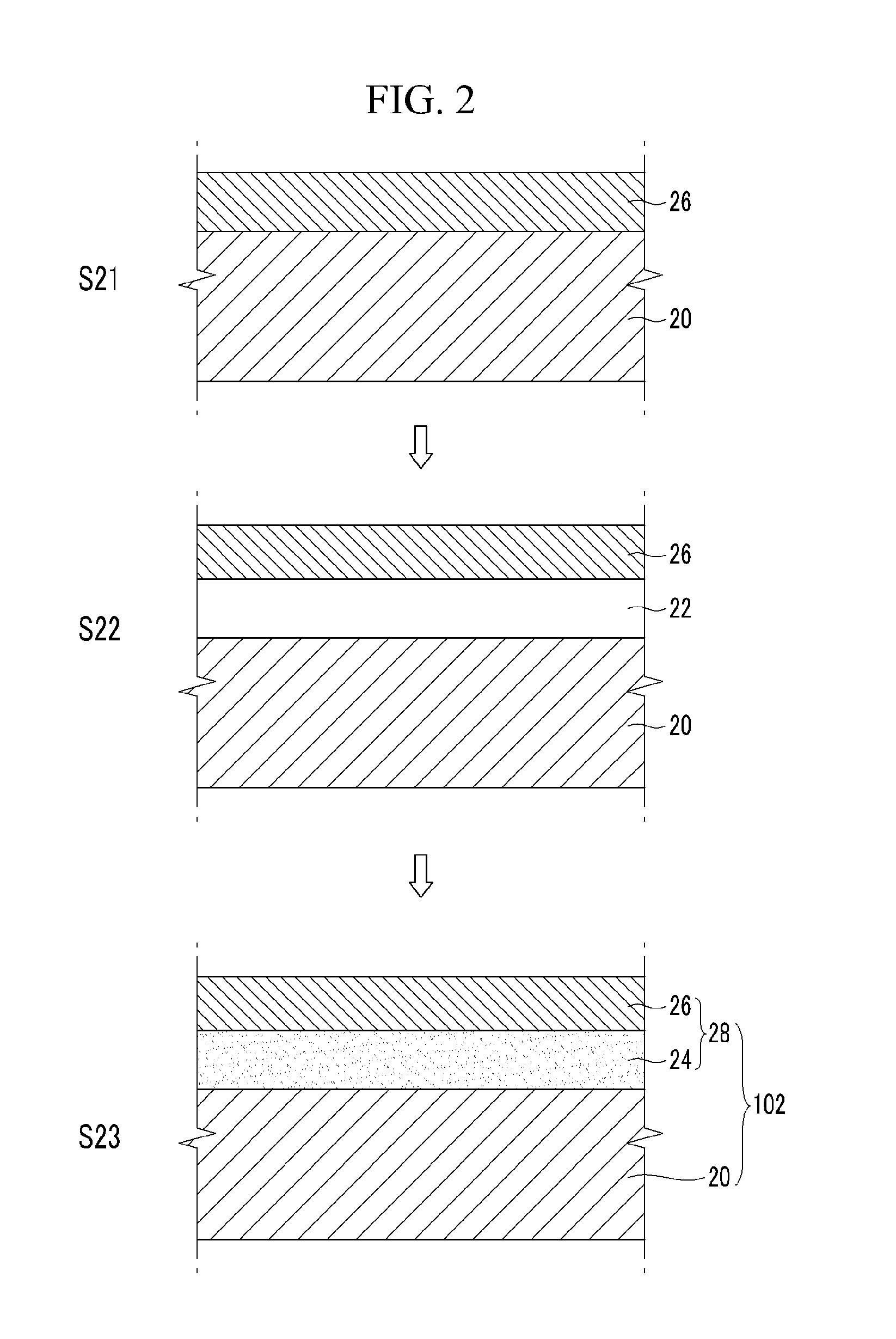
[0100]A solar cell is manufactured by substantially the same method as in Example 1, except that a clean oxidation process is further conducted after conducting the heat treatment process 1 to 5 times.
[0101]The clean oxidation process is conducted while supplying a reaction gas containing oxygen gas and hydrogen chloride gas (100 / 1 weight ratio) at a temperature of about 950° C. and under pressure of about 7.5 Torr for about 125 seconds.
[0102]Vocs of the solar cells according to Examples 1 and 2 are measured and are shown in FIG. 6. As shown in FIG. 6, it can be seen that Voc of Example 2 wherein a clean oxidation process is conducted is improved compared to Example 1. While there is some small discrepancy between the measurements of Example 1 illustrated in FIGS. 5 and 6, such discrepancies are due to minor statistical aberrations in the second set of measurements that results in slightly different measurements.
PUM
| Property | Measurement | Unit |
|---|---|---|
| temperature | aaaaa | aaaaa |
| pressure | aaaaa | aaaaa |
| temperature | aaaaa | aaaaa |
Abstract
Description
Claims
Application Information