Thin film transistor

a transistor and film technology, applied in the field of thin film transistors, can solve the problems of low field-effect mobility, etc., and achieve the effects of low current, high current, and high field-effect mobility

Inactive Publication Date: 2011-06-23
SEMICON ENERGY LAB CO LTD
View PDF100 Cites 35 Cited by
  • Summary
  • Abstract
  • Description
  • Claims
  • Application Information

AI Technical Summary

Benefits of technology

[0026]As described above, a thin film transistor with low off current, high on cu

Problems solved by technology

In formation of a thin film transistor in which a channel is formed using an amorphous silicon layer, problems such as low field-effect mobility and low on current arise.
On the other hand, a thin film transistor in which a channel is formed using a microcrystalline silicon layer has a problem in that, whereas the field-effect mobility is higher than that of the thin film transistor in which a channel is formed using an amorphous silicon layer, off current is high, and thus sufficient switching characteristics cannot be obtained.
However, formation of t

Method used


Image

  • Thin film transistor
  • Thin film transistor
  • Thin film transistor

Examples


embodiment 1

[0050]In this embodiment, a thin film transistor according to an embodiment of the present invention will be described with reference to FIGS. 1A to 1D. Note that an n-channel thin film transistor has higher carrier mobility than a p-channel thin film transistor. Further, it is preferable that all thin film transistors formed over one substrate have the same polarity because the number of manufacturing steps can be reduced. Thus, in this embodiment, an n-channel thin film transistor will be described.

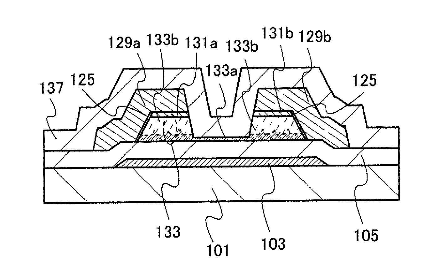
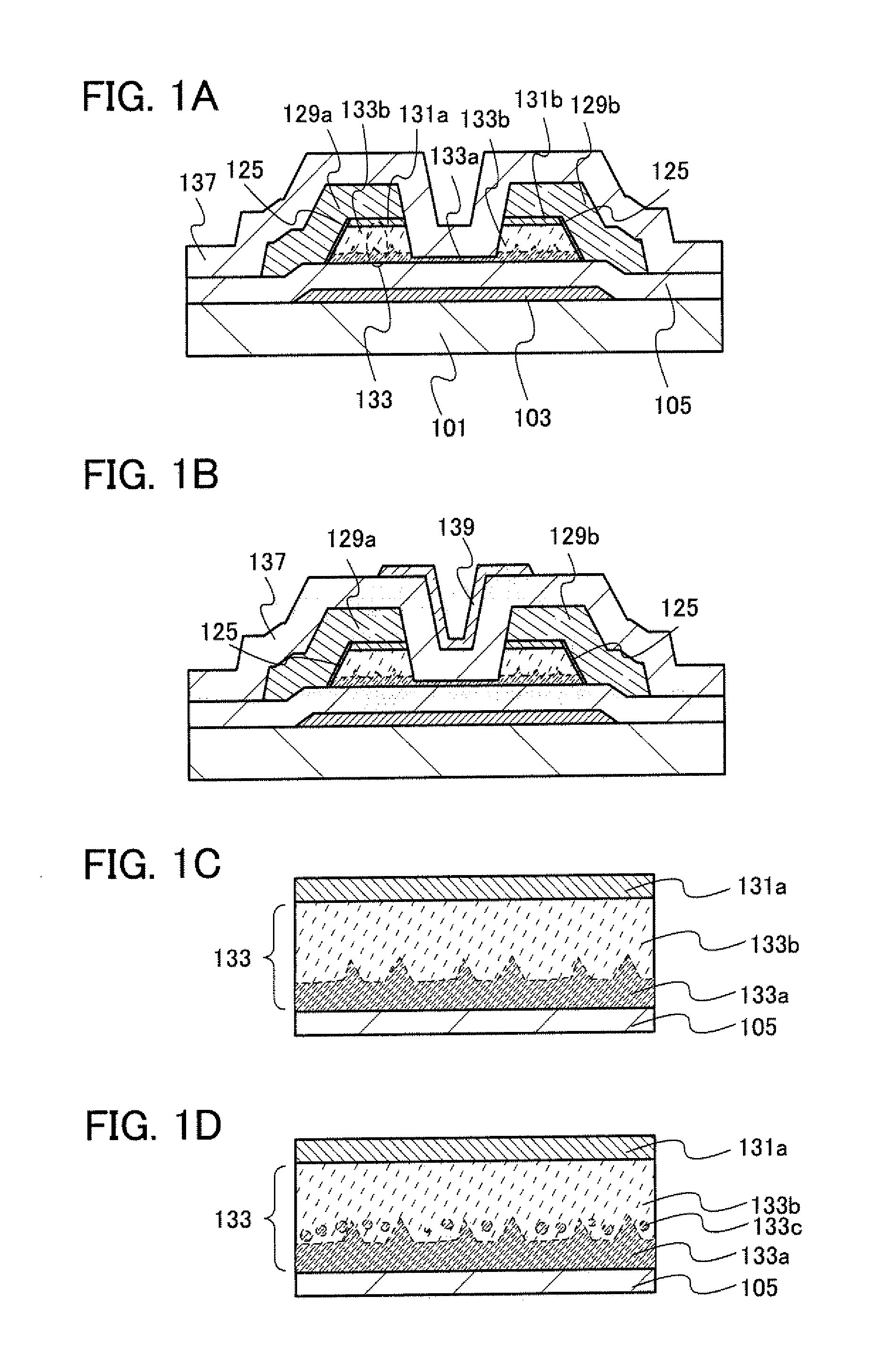
[0051]FIGS. 1A to 1D are cross-sectional views illustrating a thin film transistor described in this embodiment.

[0052]A thin film transistor illustrated in FIG. 1A includes, over a substrate 101, a gate electrode 103, a semiconductor layer 133, a gate insulating layer 105 provided between the gate electrode 103 and the semiconductor layer 133, impurity semiconductor layers 131a and 131b which are in contact with the semiconductor layer 133 and function as a source region and a drain reg...

embodiment 2

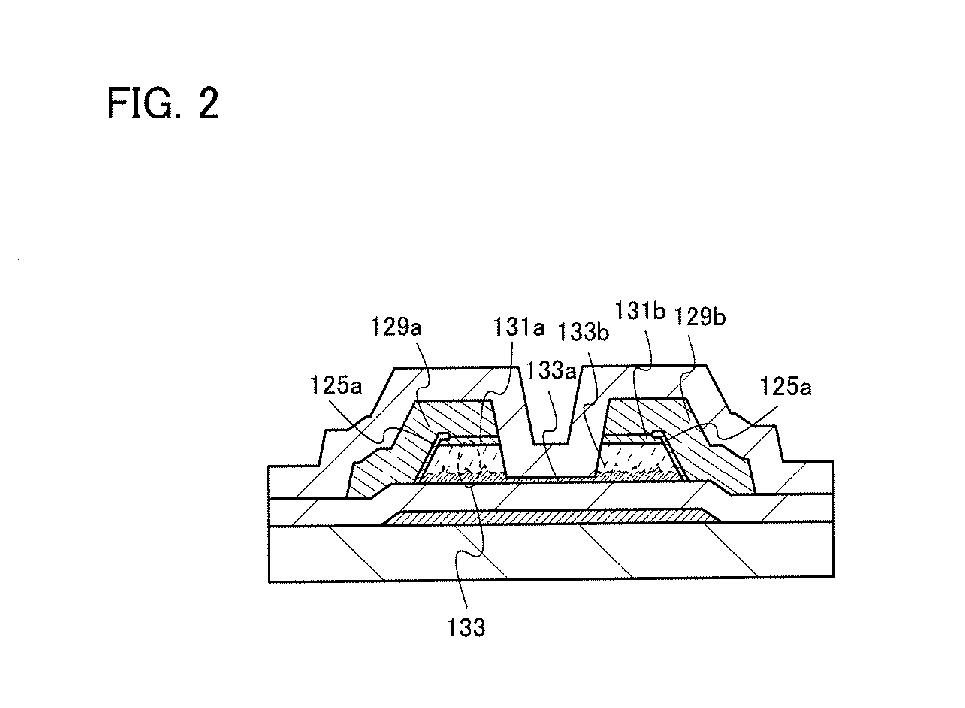
[0093]In this embodiment, a thin film transistor having a structure different from that of Embodiment 1 will be described with reference to FIGS. 4A to 4C. A difference between this embodiment and Embodiment 1 is in the barrier region.

[0094]A thin film transistor illustrated in FIG. 4A includes, over the substrate 101, the gate electrode 103, the semiconductor layer 133 including the microcrystalline semiconductor region 133a and the pair of amorphous semiconductor regions 133b, the gate insulating layer 105 provided between the gate electrode 103 and the semiconductor layer 133, the impurity semiconductor layers 131a and 131b which are in contact with the semiconductor layer 133 and function as a source region and a drain region, and the wirings 129a and 129b which are in contact with the impurity semiconductor layers 131a and 131b. In addition, a first amorphous region 126a and a second amorphous region 126b are provided on the side wall of the semiconductor layer 133. Specificall...

embodiment 3

[0105]In this embodiment, a thin film transistor having a structure different from those of Embodiment 1 and Embodiment 2 will be described with reference to FIGS. 6A and 6B. A difference between this embodiment and Embodiment 1 is in the structure of the semiconductor layer.

[0106]A thin film transistor illustrated in FIG. 6A includes, over the substrate 101, the gate electrode 103, a semiconductor layer 143, the gate insulating layer 105 provided between the gate electrode 103 and the semiconductor layer 143, the impurity semiconductor layers 131a and 131b which are in contact with the semiconductor layer 143 and function as a source region and a drain region, and the wirings129a and 129b which are in contact with the impurity semiconductor layers 131a and 131b. In addition, the insulating region 125 functioning as a barrier region is provided on the side wall of the semiconductor layer 143, that is, between the semiconductor layer 143 and the wirings 129a and 129b. Moreover, the i...


PUM


Abstract

A thin film transistor having favorable electric characteristics with high productively is provided. The thin film transistor includes a gate insulating layer covering a gate electrode, a semiconductor layer in contact with the gate insulating layer, an impurity semiconductor layer which is in contact with part of the semiconductor layer and functions as a source region and a drain region, and a wiring in contact with the impurity semiconductor layer. The semiconductor layer includes a microcrystalline semiconductor region having a concave-convex shape, which is formed on the gate insulating layer side, and an amorphous semiconductor region in contact with the microcrystalline semiconductor region. A barrier region is provided between the semiconductor layer and the wiring.

Description

BACKGROUND OF THE INVENTION[0001]1. Field of the Invention[0002]The present invention relates to a thin film transistor, a method for manufacturing the thin film transistor, and a display device to which the thin film transistor is applied.[0003]2. Description of the Related Art[0004]As a kind of field effect transistor, a thin film transistor in which a channel region is formed in a semiconductor layer fanned over a substrate having an insulating surface is known. Techniques in which amorphous silicon, microcrystalline silicon, or polycrystalline silicon is used for the semiconductor layer used in the thin film transistor have been disclosed (Patent Documents 1 to 5). A typical application of thin film transistors is a liquid crystal display television device, in which thin film transistors are put to practical use as switching transistors for each pixel that constitutes a display screen.REFERENCEPatent Document[0005][Patent Document 1] Japanese Published Patent Application No. 200...

Claims


Application Information

Patent Timeline
IPC IPC(8): H01L29/786
CPCH01L29/66765H01L29/78678H01L29/78648H01L29/78618H01L29/04
Inventor MIYAIRI, HIDEKAZUSASAGAWA, SHINYAKURATA, MOTOMU
Owner SEMICON ENERGY LAB CO LTD
Why Eureka
Try Eureka