

Semiconductor device and method for manufacturing the same
- Summary
- Abstract
- Description
- Claims
- Application Information
AI Technical Summary
Benefits of technology
Problems solved by technology
Method used
Image

Examples
embodiment 1
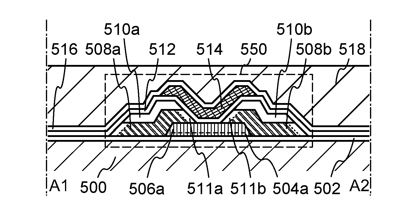
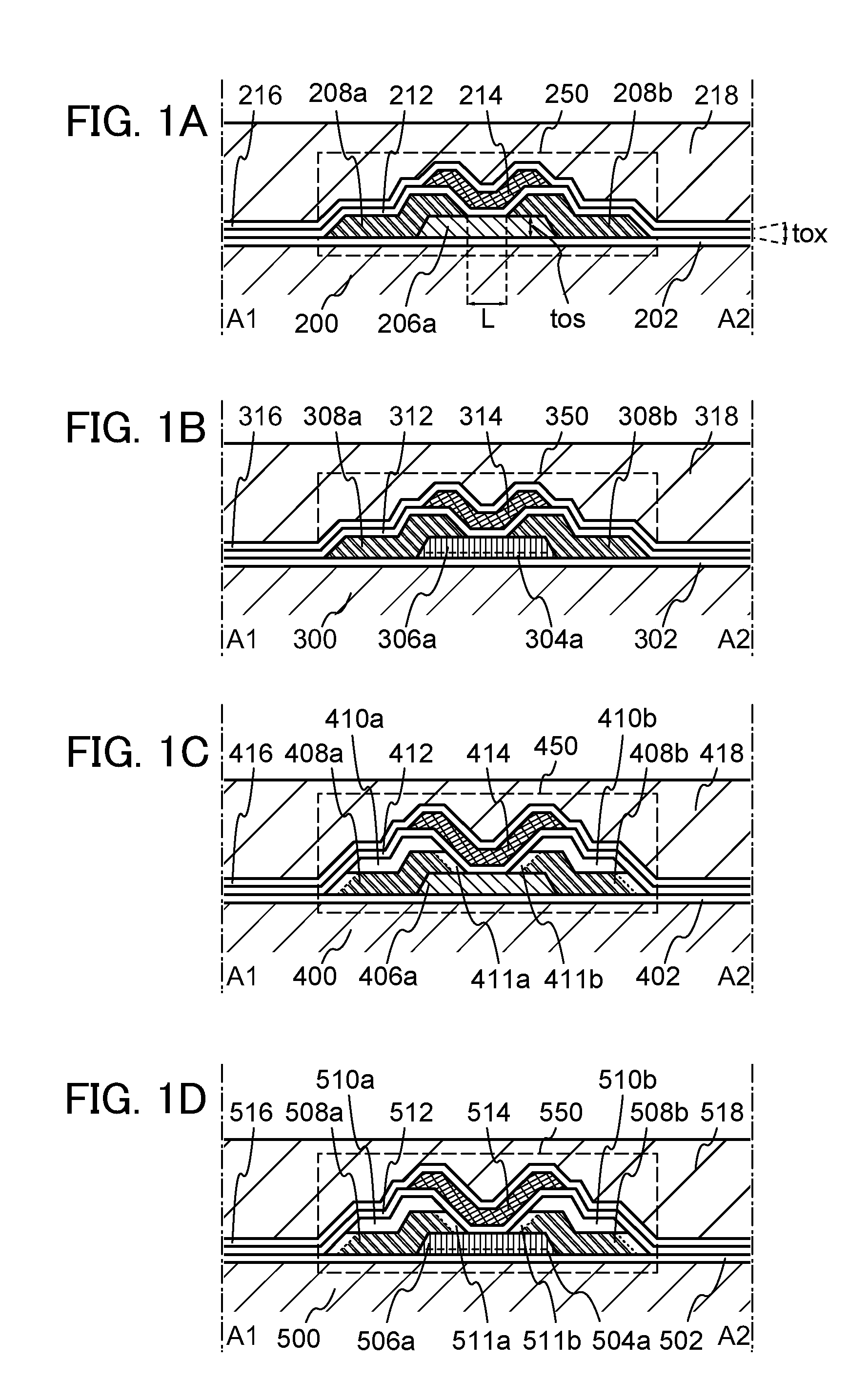
[0057]In this embodiment, a structure of a semiconductor device according to one embodiment of the disclosed invention will be described with reference to FIGS. 1A to 1D. Note that although a top-gate transistor is described as an example, the structure of a transistor is not limited to a top-gate structure.
[0058]FIG. 1A illustrates an example of a structure of a semiconductor device. A transistor 250 includes an oxide semiconductor layer 206a provided over a substrate 200; a source or drain electrode 208a and a source or drain electrode 208b electrically connected to the oxide semiconductor layer 206a; a gate insulating layer 212 provided so as to cover the oxide semiconductor layer 206a, the source or drain electrode 208a, and the source or drain electrode 208b; and a gate electrode 214 provided over the gate insulating layer 212 so as to overlap with the oxide semiconductor layer 206a. An interlayer insulating layer 216 and an interlayer insulating layer 218 are provided so as to...
embodiment 2
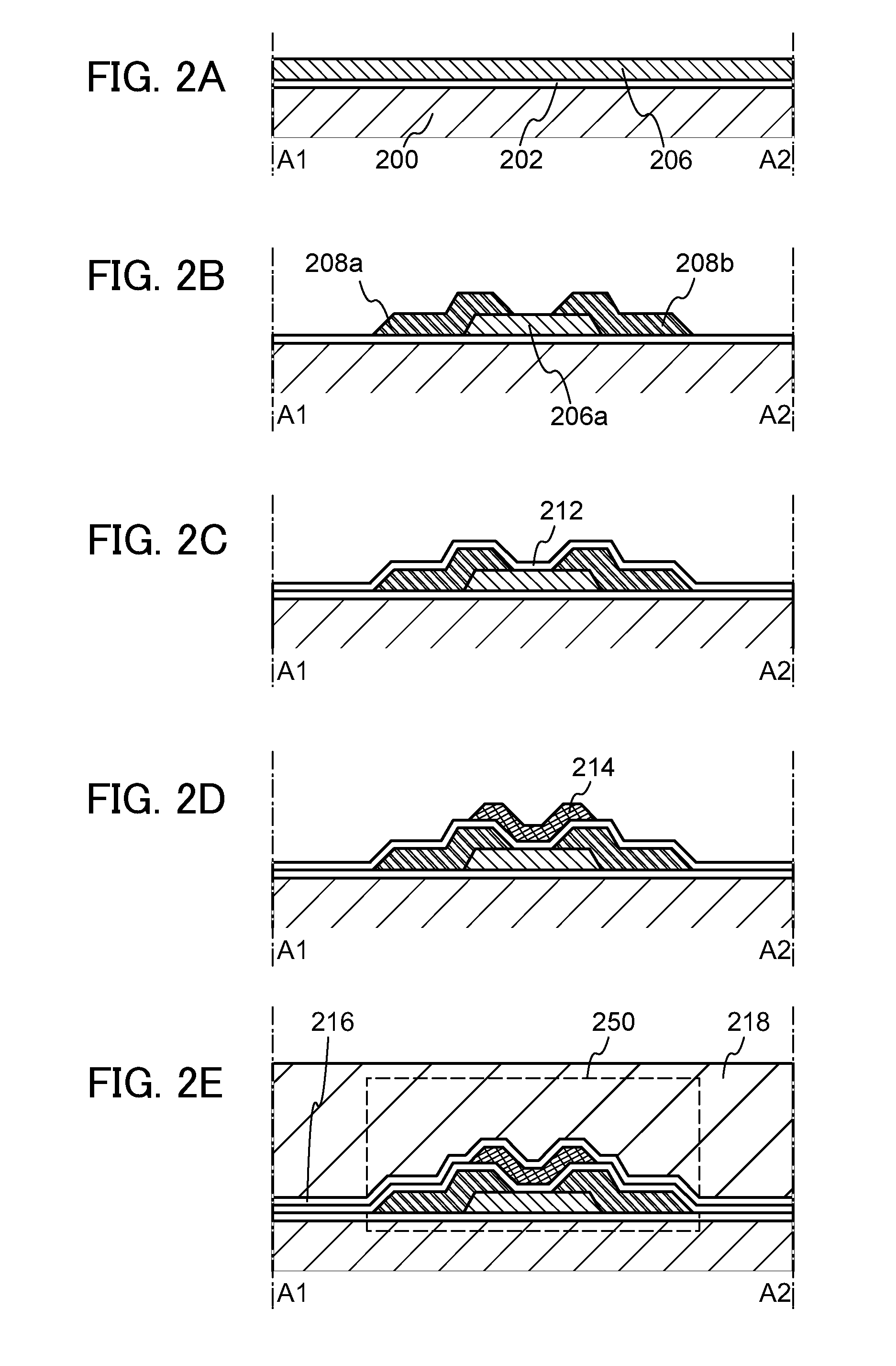
[0081]In this embodiment, a method for manufacturing a semiconductor device including an oxide semiconductor (especially, an amorphous structure) will be described. Specifically, a method for manufacturing the semiconductor device in FIG. 1A will be described with reference to FIGS. 2A to 2E. Note that although a top-gate transistor is described as an example, the structure of a transistor is not limited to a top-gate structure.
[0082]First, the insulating layer 202 is formed over the substrate 200. After that, an oxide semiconductor layer 206 is formed over the insulating layer 202 (see FIG. 2A).
[0083]As the substrate 200, for example, a glass substrate can be used. As the substrate 200, an insulating substrate formed using an insulator such as a ceramic substrate, a quartz substrate, or a sapphire substrate, a semiconductor substrate which is formed using a semiconductor material such as silicon and whose surface is covered with an insulating material, a conductive substrate which ...
embodiment 3
[0134]In this embodiment, a method for manufacturing a semiconductor device including an oxide semiconductor will be described with reference to FIGS. 3A to 3E. In this embodiment, a method for manufacturing a semiconductor device in which a first oxide semiconductor layer having a crystal region and a second oxide semiconductor layer which is formed by crystal growth from the crystal region of the first oxide semiconductor layer are used as an oxide semiconductor layer, that is, a method for manufacturing the semiconductor device illustrated in FIG. 1B will be described in detail. In the case where a required thickness can be ensured by only the first oxide semiconductor layer, the second oxide semiconductor layer is unnecessary. Note that although a top-gate transistor is described as an example, the structure of a transistor is not limited to a top-gate structure.
[0135]First, the insulating layer 302 is formed over the substrate 300. Then, a first oxide semiconductor layer is for...
PUM
 Abstract
Description
Claims
Application Information