

Method for producing build-up substrate
a technology of build-up substrate and substrate layer, which is applied in the direction of resistive material coating, nuclear engineering, railway components, etc., can solve the problems of high production cost, reduced film density of wiring material formed on catalyst pattern, and complicated production process, so as to shorten the production period, reduce production cost, and enhance the adhesion to the surface of the substrate
- Summary
- Abstract
- Description
- Claims
- Application Information
AI Technical Summary
Benefits of technology
Problems solved by technology
Method used
Image

Examples
Embodiment Construction
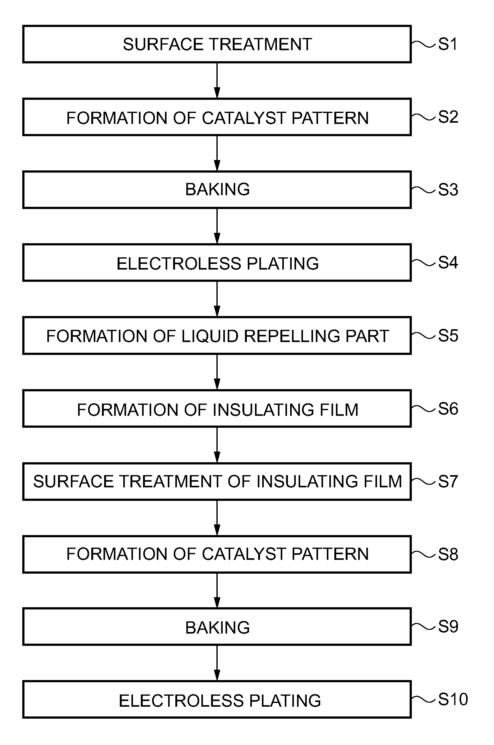
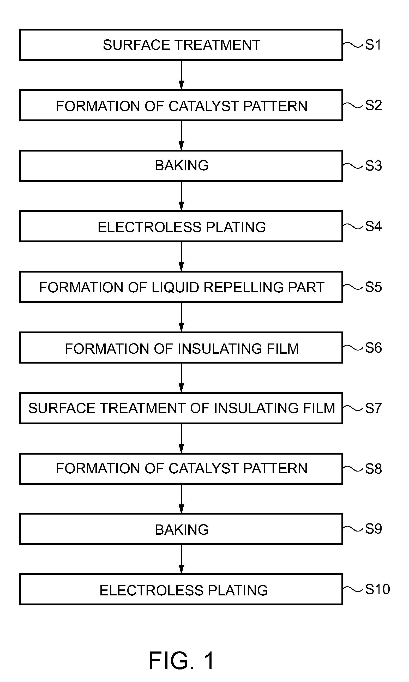
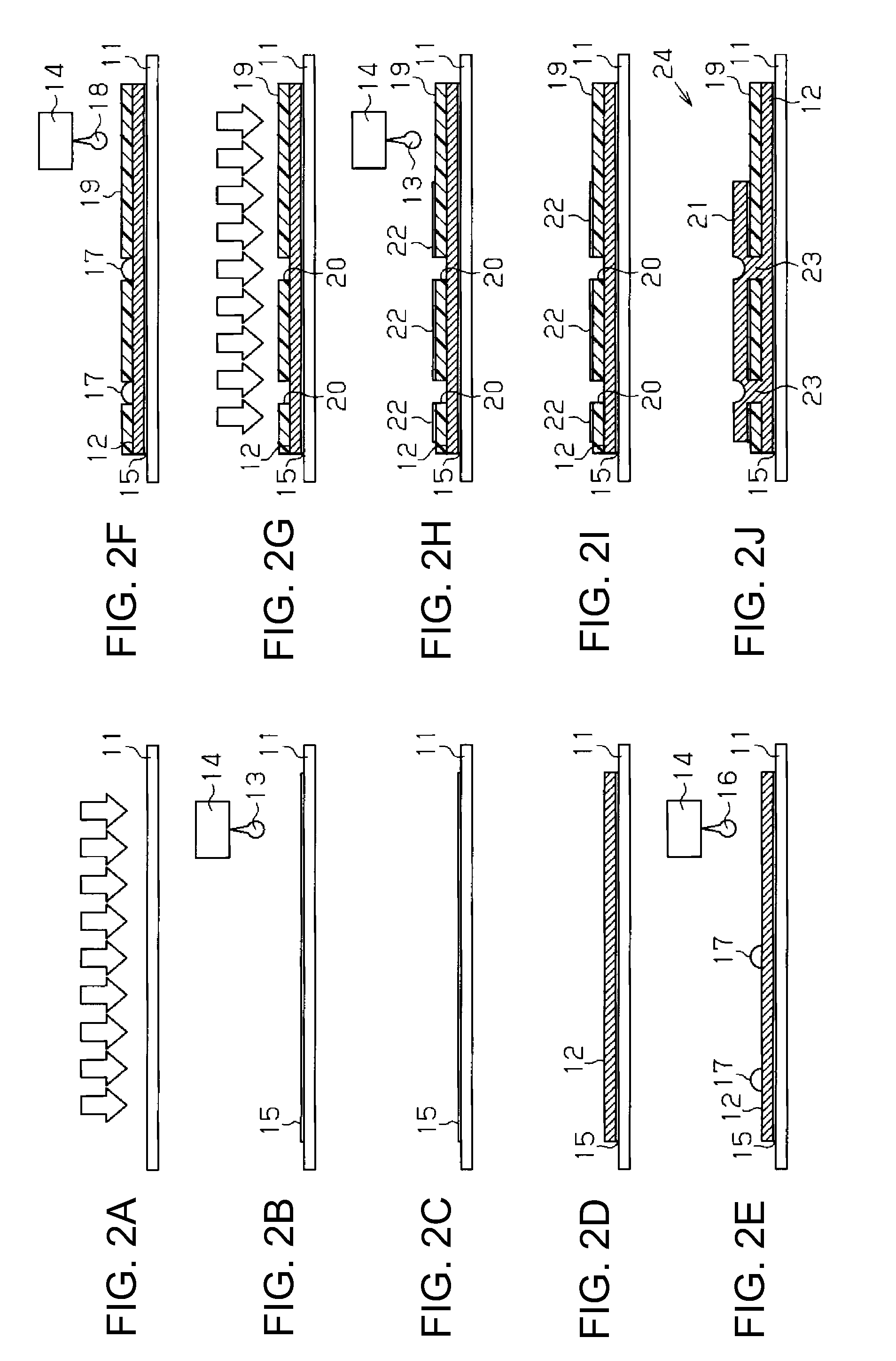
[0024]One embodiment of a method for forming a build-up substrate as one implementation of the invention will be described with reference to FIGS. 1, 2A to 2J, and 3A to 3D.
[0025]As shown in FIG. 1, the method for forming a build-up substrate according to the embodiment contains, as a process for forming a first layer wiring pattern on a substrate, surface treatment S1, formation of a catalyst pattern S2, baking S3, and electroless copper plating S4. The method for forming a build-up substrate also contains, as a process for forming a second layer wiring pattern and a contact part electrically connecting the first layer wiring pattern and the second layer wiring pattern, formation of a liquid repelling part S5, formation of an insulating film S6, surface treatment of the insulating film S7, formation of a catalyst pattern S8, baking S9, and electroless copper plating S10.
[0026]The formation of a catalyst pattern S2 and S8, the formation of a liquid repelling part S5 and the formatio...
PUM
| Property | Measurement | Unit |
|---|---|---|
| temperature | aaaaa | aaaaa |
| temperature | aaaaa | aaaaa |
| boiling point | aaaaa | aaaaa |
Abstract
Description
Claims
Application Information