
Liquid-ejecting head, liquid-ejecting apparatus, and piezoelectric element
a piezoelectric element and liquid-ejecting head technology, applied in the direction of inking apparatus, device material selection, generator/motor, etc., can solve the problems of low insulating capacity of bifeosub>3/sub>-based piezoelectric materials and generate leakage current, and achieve excellent deformation characteristics, excellent piezoelectricity, and high reliability
- Summary
- Abstract
- Description
- Claims
- Application Information
AI Technical Summary
Benefits of technology
Problems solved by technology
Method used
Image

Examples
first embodiment
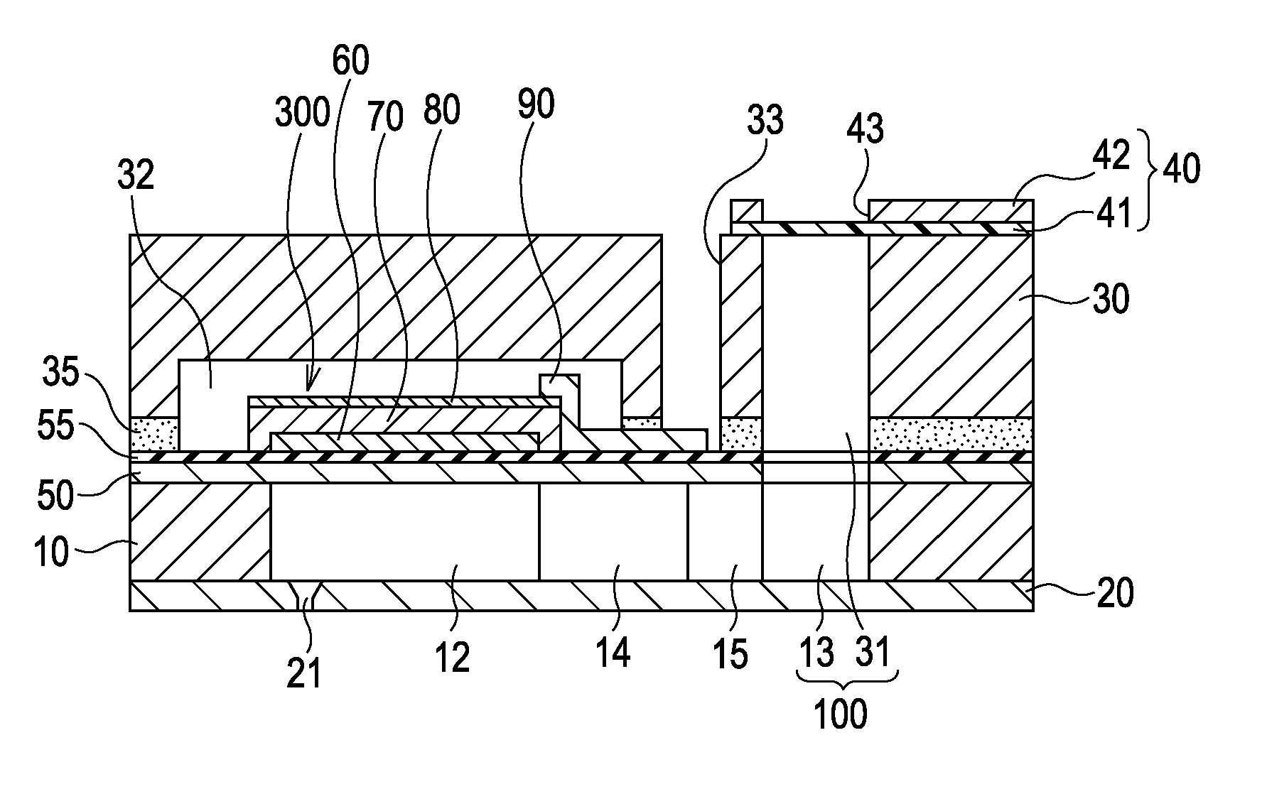
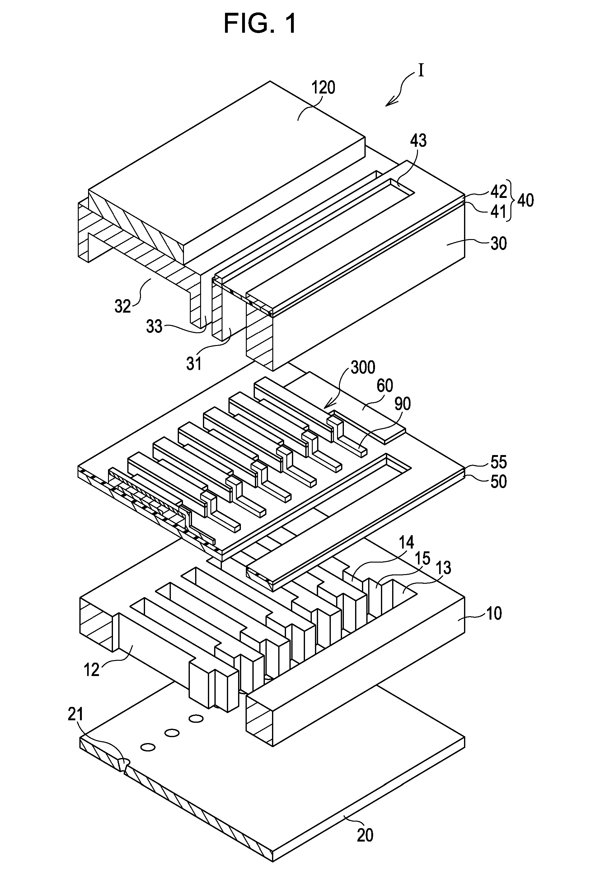
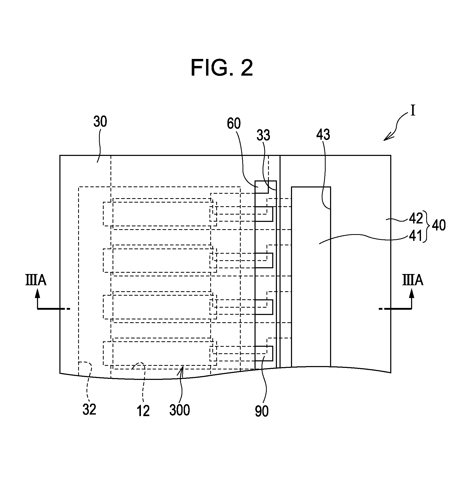
[0055]FIG. 1 is a schematic exploded perspective view of an ink jet print head as an example of a liquid-ejecting head manufactured by a method according to a first embodiment of the invention. FIG. 2 is a fragmentary plan view of the print head according to the first embodiment. FIG. 3A is a cross-sectional view of the print head taken along the line IIIA-IIIA of FIG. 2. FIG. 3B is an enlarged cross-sectional view of a principal part of the print head according to the first embodiment.
[0056]As illustrated in FIGS. 1 and 3, a flow-passage-forming substrate 10 according to the present embodiment is a silicon single crystal substrate. A silicon dioxide elastic film 50 is disposed on the flow-passage-forming substrate 10.
[0057]The flow-passage-forming substrate 10 includes a plurality of pressure-generating chambers 12 juxtaposed to each other in the width direction. The flow-passage-forming substrate 10 further includes a communication portion 13 outside the pressure-generating chambe...
example 1
[0105]A surface of a silicon substrate was thermally oxidized to form a silicon dioxide film. A zirconium oxide film having a thickness of 400 nm was then formed on the silicon dioxide film by RF sputtering. A titanium film having a thickness of 20 nm was then formed on the zirconium oxide film by DC sputtering. A platinum film having a thickness of 130 nm was then formed on the titanium film by DC sputtering.
[0106]A piezoelectric layer was then formed on the platinum film by spin coating in the following manner. First, solutions of bismuth 2-ethylhexanoate, lanthanum 2-ethylhexanoate, iron 2-ethylhexanoate, or manganese 2-ethylhexanoate in xylene and octane were mixed at a predetermined ratio to prepare a precursor solution. The precursor solution was dropped onto the substrate on which the platinum film was disposed. The substrate was initially rotated at 500 rpm for five seconds and subsequently 1500 rpm for 30 seconds to form a piezoelectric precursor film (a coating step). Dryi...
example 2
[0108]A piezoelectric element according to Example 2 was formed in the same manner as in Example 1 except that a lanthanum nickel oxide (LNO) layer having a thickness of 50 nm was formed on a platinum film by RF sputtering. For comparison purposes, a piezoelectric element including a LNO layer having a thickness of 10 nm was also fabricated.
PUM
 Abstract
Description
Claims
Application Information