

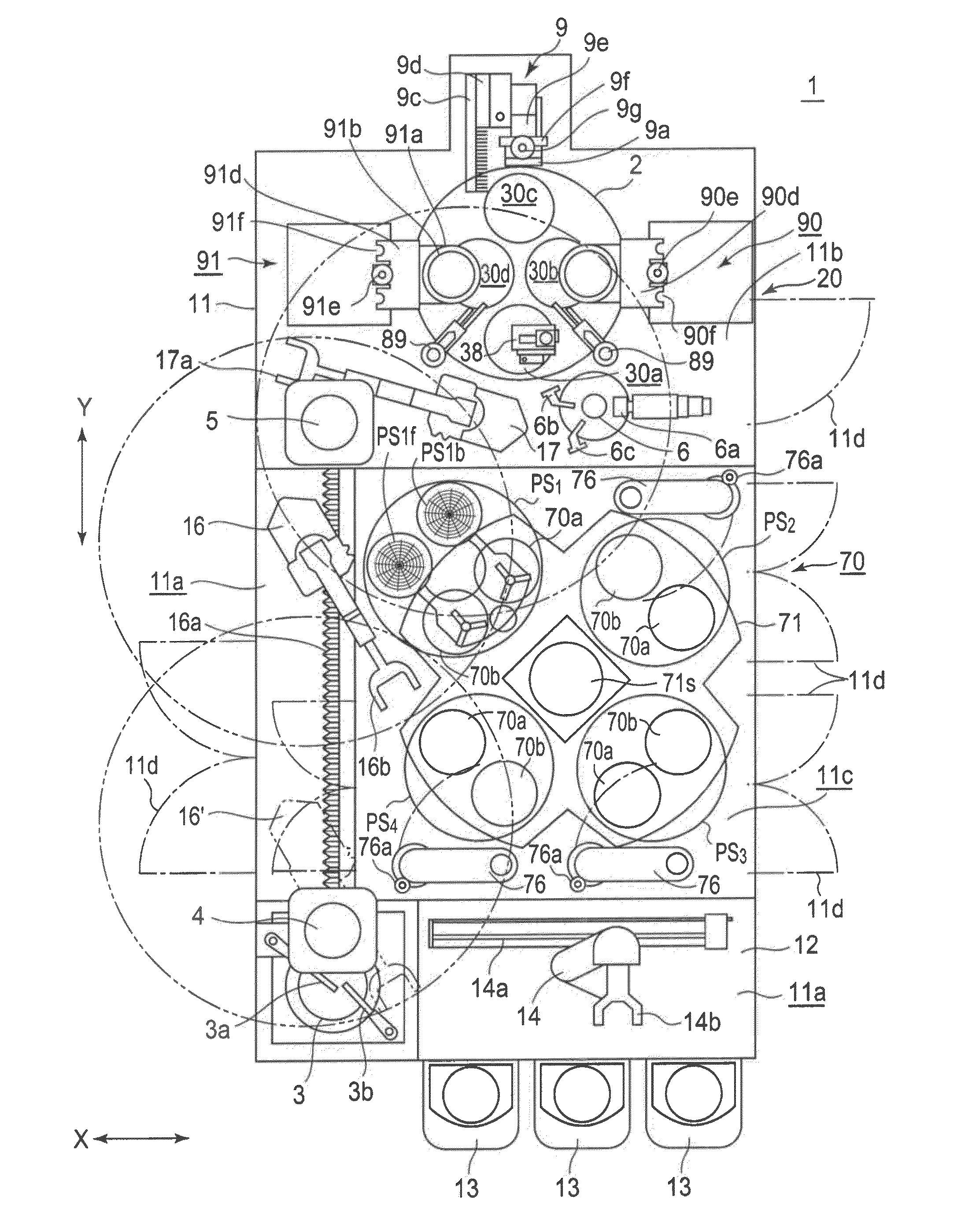
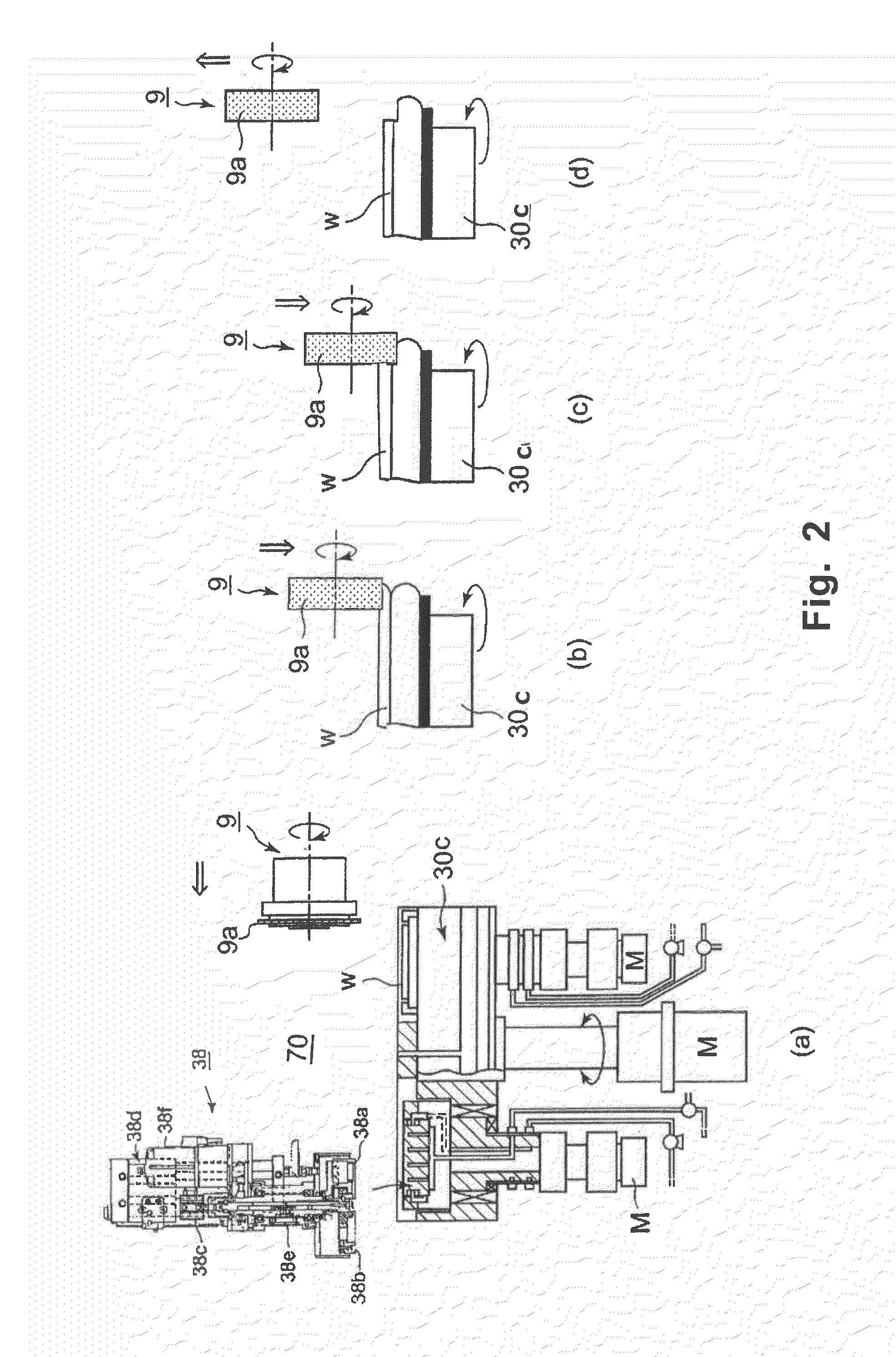
Semiconductor substrate planarization apparatus and planarization method
a semiconductor substrate and substrate technology, applied in the direction of grinding machine components, manufacturing tools, lamination machines, etc., can solve the problems of difficult chamfering of the edge portion (including the bevel portion) of the lamination bonding section of a wafer, and the presence of a grinding swarf often becomes a fatal defect, so as to accelerate the polishing
- Summary
- Abstract
- Description
- Claims
- Application Information
AI Technical Summary
Benefits of technology
Problems solved by technology
Method used
Image

Examples
embodiment 1
[0119]The substrate planarization apparatus shown in FIG. 1 was used to planarize the copper electrode head projections of the copper through-silicon substrate (TSV wafer; thickness: 1,550 μm) of a TSV wafer formed by laminating the through-electrode wafers of two substrates with a 300-mm diameter and a 775-μm thickness, under the processing conditions listed below. Table 1 lists the height distribution (unit: gm) of the copper electrode head projections in the electrode isolated part and the electrode dense part of a TSV wafer. During the planarization of the copper electrode head projections of 26 TSV wafers, no TSV wafer chipping or breakage was observed.
[0120]Process Conditions:
[0121]Rough-grinding process machining allowance: 700-μm thickness
[0122]Edge grinding machining allowance: 2 mm wide and 50 μm thick, from peripheral edge to center
[0123]Finish-grinding process machining allowance: 33-μm thickness
[0124]Rough-polishing process and medium-finish polishing process machining ...
embodiments 2 and 3
[0143]The copper electrode head projections of a through-copper-electrode silicon substrate (TSV wafer) were planarized as in Embodiment 1, except that the machining allowance of the TSV silicon substrate surface was performed under the processing conditions listed in Table 1. The distribution of the obtained heights (μm) of the copper electrode head projections of the TSV wafers is listed in Table 1.
TABLE 1GrindingPolishingMachiningMachiningElectrodeElectrodeAllowanceAllowanceIsolated PartDense PartEmbodiment(μm)(μm)ThroughputEdgeCenterEdgeCenter1733125 min. 46 sec.10.6111.805.335.622740209 min. 52 sec.18.7319.3710.5611.48375574 min. 39 sec.5.266.553.493.83
embodiment 4
[0144]The substrate planarization apparatus shown in FIG. 1 was used to planarize the rear-surface silicon substrate of a DRAM substrate formed by adhering an adhesive protective sheet to the printed wiring plane of the semiconductor substrate (diameter: 300 mm, thickness: 775 μm), a silicon substrate, under the processing conditions listed below. The average surface roughness Ra of the DRAM having an obtained silicon substrate thickness of 25 μm was 0.5 nm.
[0145]Furthermore, the average roughnesses of the ground silicon substrate surface after grinding is completed and it is moved to the polishing stage are a 4-nm Ra, 0.024-μm Ry, and 0.016-μm Rz.
[0146]No DRAM chipping or breakage was observed during planarization of the rear surface of 26 DRAMs. The throughput time per DRAM was 4 min. 42 sec.
[0147]Process Conditions:
[0148]Rough-grinding process machining allowance: 540-μm thickness
[0149]Edge grinding machining allowance: 2 mm wide and 210 μm thick, from peripheral edge to center
[0...
PUM
| Property | Measurement | Unit |
|---|---|---|
| Fraction | aaaaa | aaaaa |
| Fraction | aaaaa | aaaaa |
| Thickness | aaaaa | aaaaa |
Abstract
Description
Claims
Application Information