Plasma processing apparatus and method

a processing apparatus and plasma technology, applied in the direction of plasma technique, chemical vapor deposition coating, coating, etc., can solve the problems of difficult uniform conversion of difficult to uniformly convert processing gas into plasma, and high current current flowing between the mounting table and the gas shower head, etc., to achieve high in-plane uniformity

Active Publication Date: 2011-07-21
TOKYO ELECTRON LTD
View PDF11 Cites 194 Cited by
  • Summary
  • Abstract
  • Description
  • Claims
  • Application Information

AI Technical Summary

Benefits of technology

[0016]In view of the above, the present invention provides a plasma processing apparatus and a plas...

Problems solved by technology

However, in the CCP processing method, a path of a current flowing between the mounting table and the gas shower head is extremely complicated.
Thus, it is difficult to uniformly convert the processing gas into the plasma, and the plasma density on the surface of the wafer is apt to be non-uniform.
Further, in this method, a high electron temperature of the plasma may inflict damages on the wafer.
Moreover, a high frequency power supply needs to be connected to both or one of the mounting table and the gas shower head and, hence, the cost of the apparatus is increased.
However, when the coil is installed on the gas shower head formed of a metal which is provided at the ceiling wall of the processing chamber, the electric field is blocked by the gas shower head.
Therefore, in order to form the uniform electric field in the processing region, the shower head formed of a metal cannot be used.
However, a dielectric material, e.g., quartz, has poor workability compared to a metal, so that it is difficult to form the gas shower head by using the dielectric material in view of workability.
Moreover, since the concentration of the processing gas is non-uniform near the ceiling wall or the sidewall of the processing chamber, a large gap needs to be provided between the wafer (mounting table) and the ceiling wall or the sidewall of the processing chamber in order to improve the concentration distribution of the processing gas near the wafer.
However, this results in scaling up of the processing chamber.
Further, when the ceiling wall of the processing chamber is formed of a dielectric material, e.g., quartz, it is difficult to form a cooling water path at the ceiling wall in view of workability and, hence, it is difficu...

Method used


Image

  • Plasma processing apparatus and method
  • Plasma processing apparatus and method
  • Plasma processing apparatus and method

Examples


Embodiment Construction

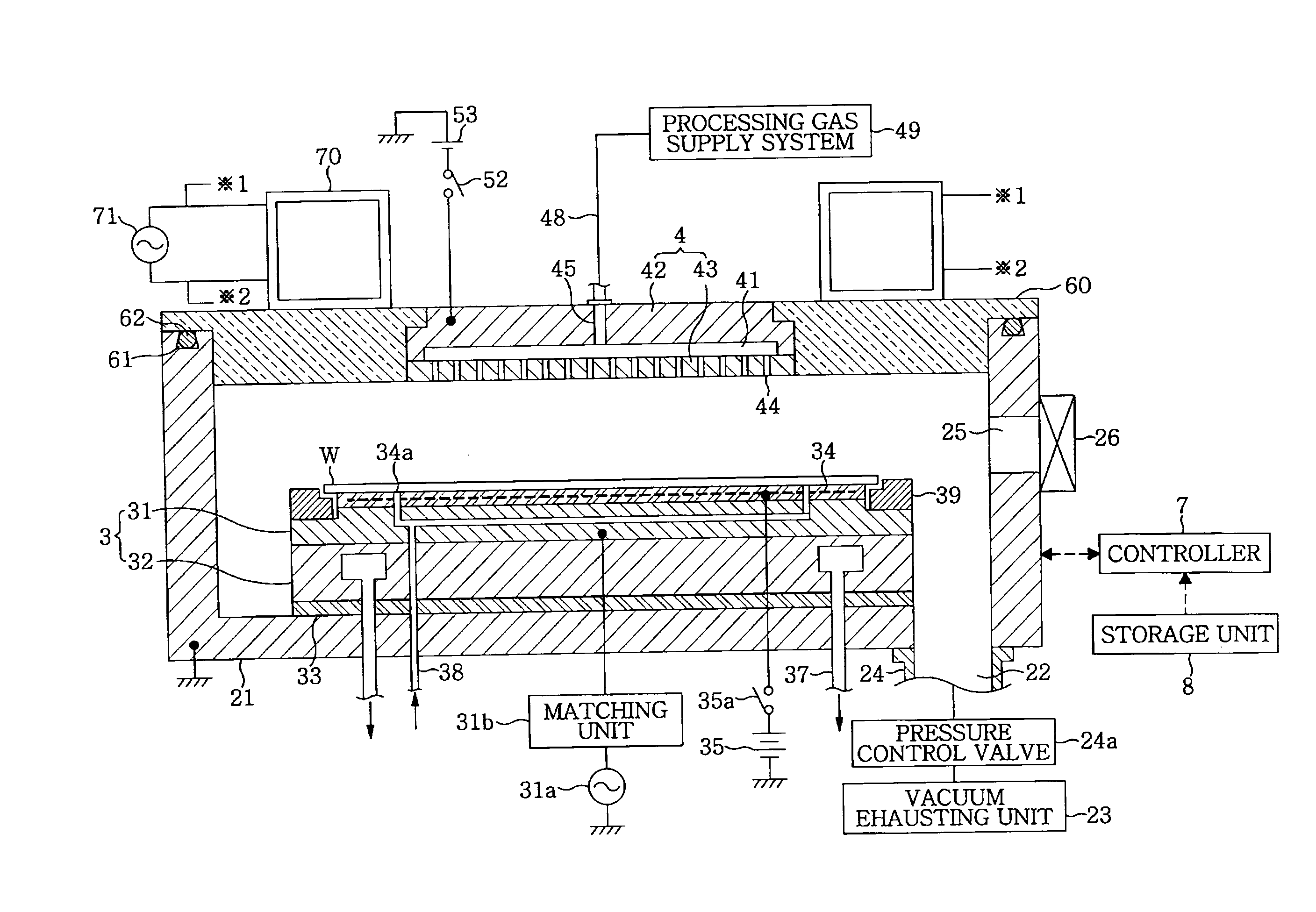
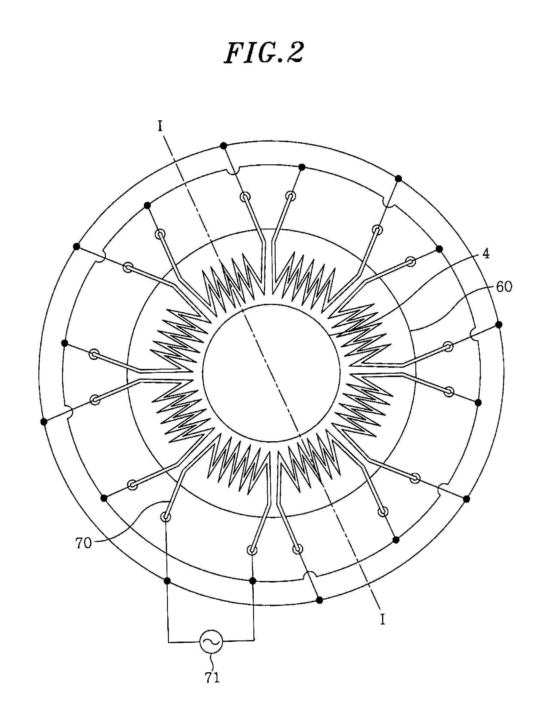
[0079]A plasma processing apparatus in accordance with a first embodiment of the present invention will be described with reference to FIGS. 1 to 5. This plasma processing apparatus performs a plasma process, e.g., an etching process, on a semiconductor wafer (hereinafter, referred to as a “wafer”) as a substrate by a plasma of a processing gas. The following is brief description of the wafer W. The wafer W has a silicon base film and films laminated thereon. The laminated films include a photoresist mask formed of, e.g., an organic material, and having a predetermined pattern, a bottom anti-reflection coating film formed of, e.g., an organic film, an amorphous carbon film, an insulating film (SiO2 film or SiCOH film) or a Poly-Si (polycrystalline silicon) film, an etching stop film formed of, e.g., an inorganic film, and the like, which are laminated in that order from the top. As will be described later, the plasma processing apparatus performs an etching process to form a recess ...


PUM


Abstract

A plasma processing apparatus performs a process on a substrate by using plasma. The plasma processing apparatus includes a processing chamber; a mounting table which is located in the processing chamber and on which a substrate is mounted; a gas shower head formed of a conductive material provided to face the mounting table and having at the bottom surface thereof a plurality of gas injection openings for supplying a processing gas into the processing chamber; an induction coil to which a high frequency current is supplied to generate an inductively coupled plasma in a region surrounding a space below the gas shower head; a negative voltage supplying unit for applying a negative DC voltage to the gas shower head to allow an electrical field, which is induced by the induction coil, to be drawn to a central portion of the processing region; and a unit for evacuating the processing chamber.

Description

FIELD OF THE INVENTION[0001]The present invention relates to a plasma processing apparatus and a plasma processing method for performing a plasma process on a substrate.BACKGROUND OF THE INVENTION[0002]A semiconductor device manufacturing process includes a step for performing a plasma process such as an etching process, a film forming process or the like on a surface of a semiconductor wafer (hereinafter, referred to as a “wafer”) as a substrate by using a plasma.[0003]For example, an etching process is performed on multilayer films having different compositions, e.g., a bottom anti-reflection coating film, an amorphous carbon film, a silicon oxide film, an etching stop film and the like, which are laminated below a pattern mask in that order from the top on an silicon film of a pattern mask. Therefore, when a recess is formed in these multilayer films, an etching gas is changed for each film and, also, processing conditions such as a flow rate of the etching gas, a pressure and th...

Claims


Application Information

Patent Timeline
IPC IPC(8): C23F1/00C23F1/08C23C16/455C23C16/458C23C16/50C23C16/511C23C16/52
CPCH01J37/32091H05H1/46H01J37/32165H01J37/321H01L21/3065
Inventor SAWADA, IKUOKANG, SONGYUNKASAI, SHIGERU
Owner TOKYO ELECTRON LTD
Why Eureka
Try Eureka