Preparing large-sized emitting colloidal nanocrystals

a colloidal solution and nanocrystal technology, applied in the direction of chemistry apparatus and processes, light emitting compositions, etc., can solve the problems of poor efficiency, poor efficiency, poor efficiency, etc., and achieve high emission efficiency, narrow size distribution, and crystallinity high

Inactive Publication Date: 2011-07-21
EASTMAN KODAK CO
View PDF1 Cites 25 Cited by
  • Summary
  • Abstract
  • Description
  • Claims
  • Application Information

AI Technical Summary

Benefits of technology

[0019]It is an advantage of the present invention to enable a method of making a colloidal solution of large-sized emitting nanocrystals, wherein each emitting nanocrystal includes a core structure wherein the cores have aspect ratio less than 2:1 and a diameter greater than 10 nanometers and a protective shell surrounding the core.
[0020]It is also an advantage of the present invention that the colloidal ternary nanocrystals made in accordance with the present method exhibit the desirable properties of high crystallinity, narrow size distribution, high emission efficiency, ability to form polycrystalline films with less than 5% by volume of organic material, high temperature stability, stable fluorescence after removal of organic passivating ligands, and robustness for high temperature anneals.
[0021]Another advantage of the present invention is that the large-sized emitting colloidal nanocrystals exhibiting these properties can be used to create advantaged quantum dot phosphors, medical and biological sensors, high efficiency LEDs and lasers.

Problems solved by technology

Because of problems, such as, aggregation of the quantum dots in the emitter layer, the efficiency of these devices was rather low in comparison with typical OLED devices.
The efficiency was even poorer when a neat film of quantum dots was used as the emitting layer (Hikmet et al., J. Appl. Phys. 93, 3509 (2003)).
The poor efficiency was attributed to the insulating nature of the quantum dot layer.
Regardless of any future improvements in efficiency, these hybrid devices still suffer from all of the drawbacks associated with pure OLED devices.
The resulting device had a poor external quantum efficiency of 0.001 to 0.01%.
These organic ligands are insulators and would result in poor electron and hole injection into the quantum dots.
In addition, the remainder of the structure is costly to manufacture, due to the usage of electron and hole semiconducting layers grown by high vacuum techniques, and the usage of sapphire substrates.
Despite these advantages, quantum dot phosphors have not been introduced into the marketplace due to some major shortcomings; such as, poor temperature stability and insufficient (10-30%) quantum yields for phosphor films with high quantum dot packing densities.
The disadvantage of this approach is that the resulting quantum dot phosphor films are unacceptably thick (1 mm), as compared to the desired thickness of 10 μm.
A major problem encountered over the years in fabricating high quality colloidal nanocrystals is associated with materials issues, primarily the tendency to form defects and surface trap states under the employed growth conditions, resulting in low luminescence efficiency and insufficient stability.
Organic passivation is often incomplete and reversible.
However, for the largely mismatched core-shell structures, the interface strain accumulates dramatically with increasing shell thickness, and eventually can be released through the formation of misfit dislocations, degrading the optical properties of the QDs.
This limits their functionality in biomedical labeling and electronic device applications.
However, it has been shown that it is not an easy task to grow colloidal nanocrystals having sizes larger than 5 nm while maintaining the emission intensity.
This is because significant amounts of defects are formed as the size becomes larger, which act as the emission quencher.
However, many applications also demand nanocrystals that are not only robust but also insensitive to their surface chemistry and surface conditions.
It has been demonstrated by our group and others that regular-sized (˜5 nm) nanocrystals are often inadequate meeting all the requirements.
To date, optoelectronic devices or biological (medical) studies have not had emitting colloidal nanocrystals available that have a size larger than 10 nm before the shelling steps.
The synthesis took 5 days, and the nanocrystals suffer from wide size distributions and low PL efficiencies.

Method used


Image

  • Preparing large-sized emitting colloidal nanocrystals
  • Preparing large-sized emitting colloidal nanocrystals
  • Preparing large-sized emitting colloidal nanocrystals

Examples


example 1

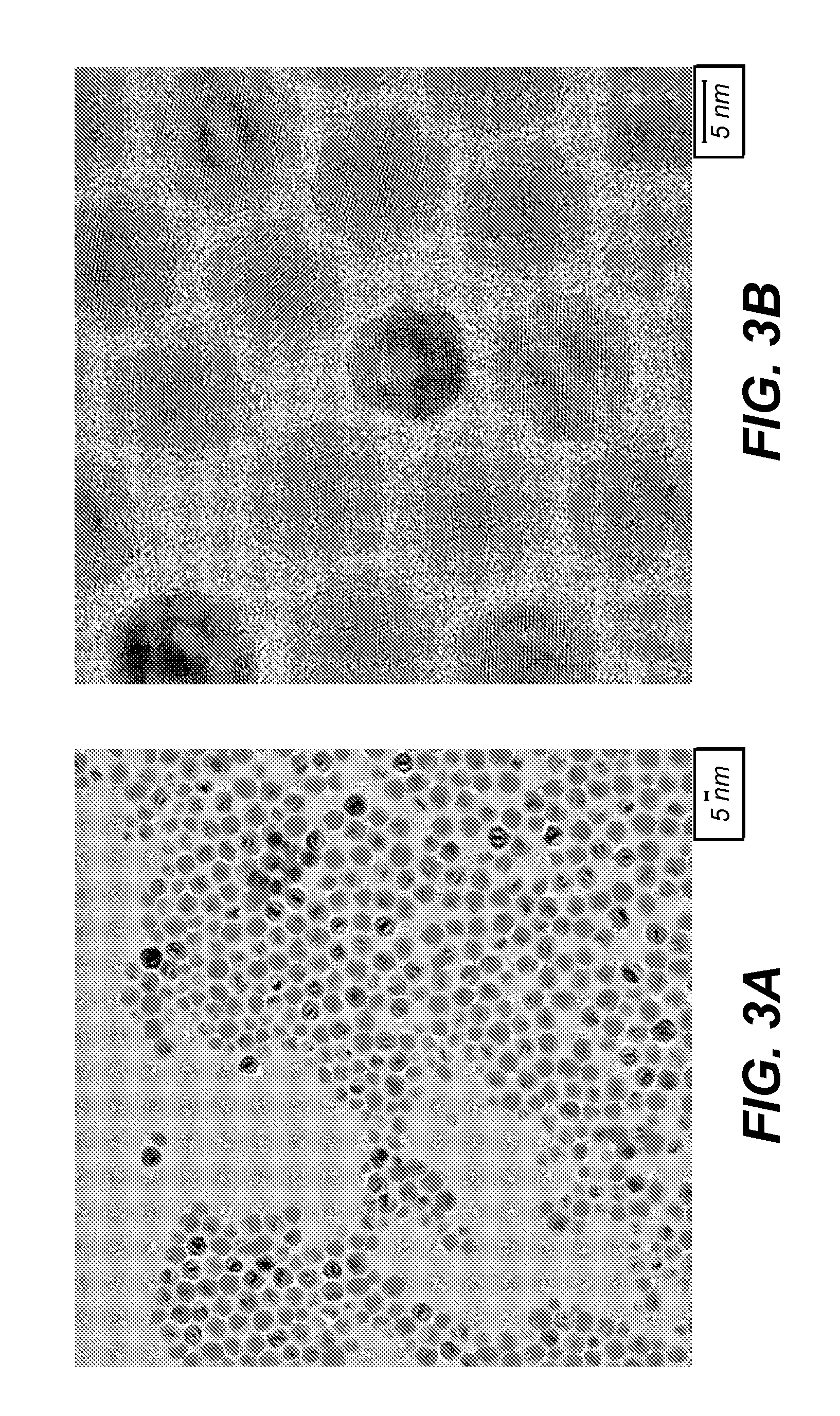
[0073]The cadmium precursor is cadmium acetate, the zinc precursor is Zn(Et)2, and the selenium precursor is TOPSe. The coordinating solvent for the growth is a mixture of trioctylphosphine oxide (TOPO), trioctylphosphine (TOP) and stearic acid. TOPO and TOP are degassed at 190° C. for 60 minutes prior to their usage. Inside a dry box, 0.046 g (0.2 mmol) cadmium acetate and 3 g stearic acid were added into a three-neck flask. The flask was placed on a Schlenk line and vacuum was applied. The mixture went clear after heating at 100° C. for 5-10 minutes. After cooling down, the flask was transferred into the box, and 1.1 ml TOPO was added. The mixture was degassed at 100° C. for 30 minutes. After switching to argon overpressure, the flask contents were taken up to 350° C., and 1 ml TOPSe solution in TOP prepared by dissolving 0.7896 g (10 mmol) Se in 10 ml Top in the dry box was added into the solvent mixture by injection from a syringe as quickly as possible, followed by the injectio...


PUM

PropertyMeasurementUnit
diameteraaaaaaaaaa
aspect ratioaaaaaaaaaa
diameteraaaaaaaaaa

Abstract

A method of making a colloidal solution of ternary AIAIIB nanocrystals, wherein AI and AII are independently selected from an element of periodic table subgroup IIB, when B represents an element of periodic table main group VI; or AI and AII are independently selected from an element from periodic table main group III, when B represents an element of periodic table main group V. The method providing a mixture of AI in a suitable form for the generation of a nanocrystal, and coordinating solvents including at least 30 wt % of fatty acids; heating the reaction mixture for a suitable time, adding B in a suitable form for the generation of a nanocrystal, adding AII in a suitable form for the generation of a nanocrystals; and heating the reaction mixture for a sufficient period of time at a temperature suitable for forming nanocrystal AIAIIB.

Description

CROSS-REFERENCE TO RELATED APPLICATIONS[0001]Reference is made to commonly-assigned, co-pending U.S. patent application Ser. No. ______ (Kodak Docket 96019US01) filed concurrently herewith, entitled “DEVICE CONTAINING LARGE-SIZED EMITTING COLLOIDAL NANOCRYSTALS” by Ren et al., the disclosure of which is incorporated herein.FIELD OF THE INVENTION[0002]The present invention relates to a method of making a colloidal solution of large-sized emitting nanocrystals.BACKGROUND OF THE INVENTION[0003]A quantum dot is a semiconductor whose excitons are confined in all three spatial dimensions. As a result, it has properties that are between those of bulk semiconductors and those of discrete molecules. An immediate optical feature of colloidal quantum dots is their coloration. While the material which makes up a quantum dot defines its intrinsic energy signature, the quantum dots of the same material, but with different sizes, can emit light of different colors. The physical reason is the quant...

Claims


Application Information

Patent Timeline
Patent Type & Authority Applications(United States)
IPC IPC(8): C09K11/54C09K11/08
CPCC09K11/025C09K11/883C09K11/565
Inventor REN, XIAOFANKAHEN, KEITH B.
Owner EASTMAN KODAK CO
Why Eureka
Try Eureka