
Film of n type (100) oriented single crystal diamond semiconductor doped with phosphorous atoms, and a method of producing the same

a technology of phosphorous atoms and n-type atoms, which is applied in the direction of polycrystalline material growth, crystal growth process, transportation and packaging, etc., can solve the problems of n-type atoms added to the amount of n-type atoms, the crystallinity of the fabricated is not affected, and the film of n-type (100) oriented single crystal diamond semiconductor cannot be obtained, etc., to achieve the effect of large impact in the industry

Inactive Publication Date: 2011-07-21
KATO HIROMITSU +3
View PDF7 Cites 3 Cited by
  • Summary
  • Abstract
  • Description
  • Claims
  • Application Information

AI Technical Summary

Benefits of technology

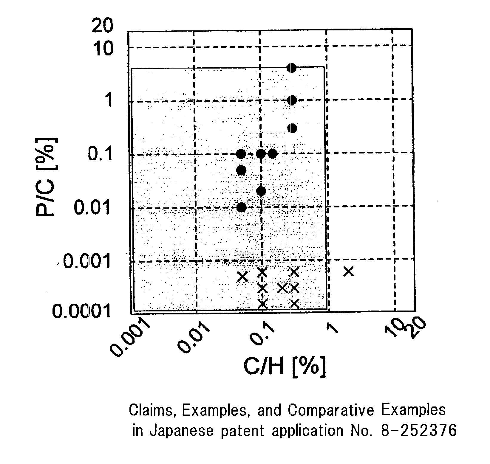
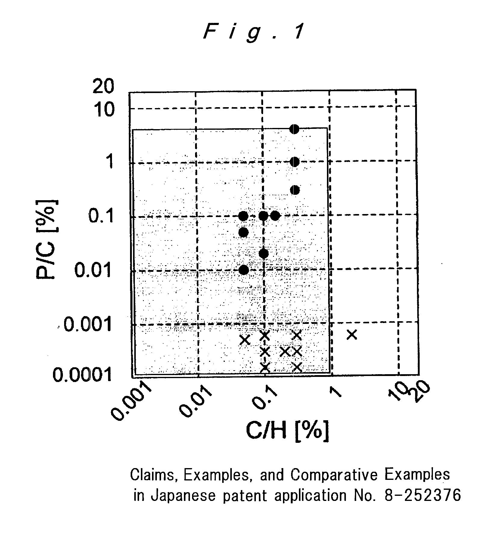
"The present invention provides a method for manufacturing a film of an n type (100) oriented single crystal diamond semiconductor doped with phosphorous atoms. By using a phosphorous vapor in a concentration at a level which deviates from common knowledge, the inventors solved the problem of doping diamond semiconductor using a plasma chemical vapor deposition method. The invention can be used with different methods of chemical vapor deposition such as microwave CVD, filament CVD, DC plasma CVD, and arc jet plasma CVD. The invention also allows for the use of a diamond substrate with an off angle of 0 degree to 10 degrees and control of the weight ratio of phosphorous atoms to carbon atoms in the plasma vapor phase to control the properties of the semiconductor. The temperature on the surface of the substrate can also be set to 800° C. to 1000° C."

Problems solved by technology

However, as far as the present inventors know, there are no preceding examples that confirmed the existence of an n type diamond semiconductor on the (100) plane in any patent or academic paper.
Even when such methods are attempted, however, a film of n type (100) oriented single crystal diamond semiconductor, which is important in the industry, could not be obtained, due to poor reactivity.
This is because it was firmly believed that increase in the amount of n type atoms added to be harmful to the crystallinity of the fabricated n type diamond semiconductor single crystal film.
The crystallinity of diamond becomes poor when the concentration is further increased.

Method used


Image

  • Film of n type (100) oriented single crystal diamond semiconductor doped with phosphorous atoms, and a method of producing the same
  • Film of n type (100) oriented single crystal diamond semiconductor doped with phosphorous atoms, and a method of producing the same
  • Film of n type (100) oriented single crystal diamond semiconductor doped with phosphorous atoms, and a method of producing the same

Examples


example 1

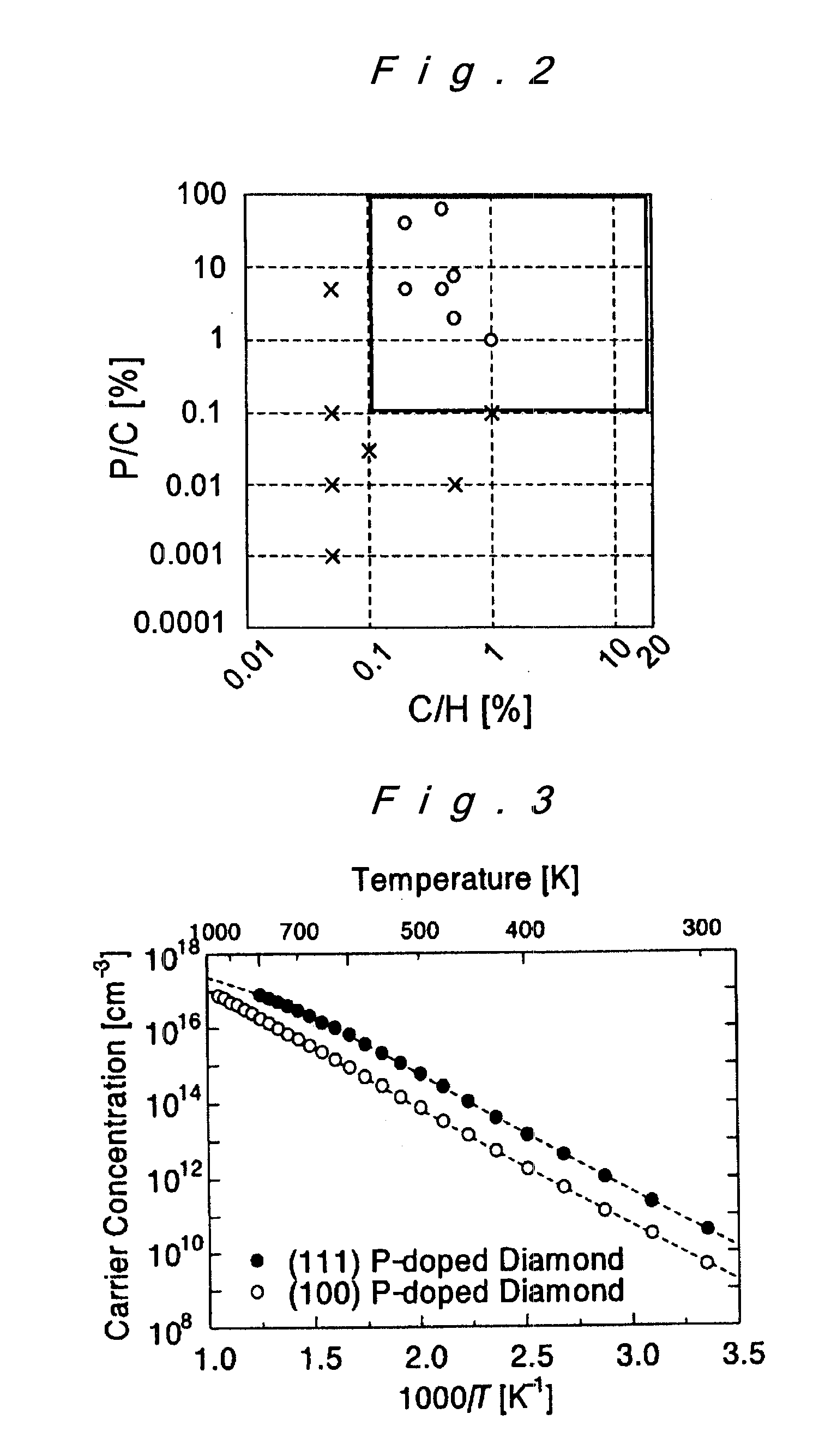
[0038]In accordance with a microwave plasma chemical vapor phase synthesizing method, phosphine was added to hydrogen containing 0.2% of methane so that the ratio of phosphorous (P) to carbon (C) became 5% and the resulting gas was introduced into a reaction chamber having a pressure for synthesis of 50 Torr, and a diamond film was formed on the (100) oriented single crystal diamond having an off angle of 1.5 degrees (a diamond substrate where the plane direction is inclined by 1.5 degrees in any direction for the (100) plane), on the substrate at 900° C. The film was confirmed to have n type properties at room temperature by measuring the Hall effect, and the mobility thereof was 350 cm2 / Vs and the concentration of the carrier was 3×109 cm−3.

example 2

[0039]In accordance with a microwave plasma chemical vapor phase synthesizing method, phosphine was added to hydrogen containing 0.5% of methane so that the ratio of phosphorous (P) to carbon (C) became 7.5% and the resulting gas was introduced into a reaction chamber kept at a pressure for synthesis of 75 Torr, and a diamond film was formed on the (100) oriented single crystal diamond having an off angle of 2.8 degrees, at 800° C. on the substrate. The film was confirmed to have n type properties at room temperature by measuring the Hall effect, and the mobility thereof was 47 cm2 / Vs and the concentration of the carrier was 9×109 cm−3.

example 3

[0040]In accordance with a microwave plasma chemical vapor phase synthesizing method, phosphine was added to hydrogen containing 0.4% of methane so that the ratio of phosphorous (P) to carbon (C) became 5% and the resulting gas was introduced into a reaction chamber kept at a pressure for synthesis of 25 Torr, and a diamond film was formed on the (100) oriented single crystal diamond having an off angle of 0.5 degrees at 900° C. of the substrate. The film was confirmed to have n type properties at room temperature by measuring the Hall effect, and the mobility thereof was 230 cm2 / Vs and the concentration of the carrier was 5×109 cm−3.


PUM

PropertyMeasurementUnit
off-angleaaaaaaaaaa
off angleaaaaaaaaaa
off angleaaaaaaaaaa

Abstract

There is provided an n type (100) oriented single crystal diamond semiconductor film into which phosphorous atoms have been doped and a method of producing the same. The n type (100) oriented single crystal diamond semiconductor film, characterized in that (100) oriented diamond is epitaxially grown on a substrate under such conditions that; the diamond substrate is (100) oriented diamond, a means for chemical vapor deposition provides hydrogen, hydrocarbon and a phosphorous compound in the plasma vapor phase, the ratio of phosphorous atoms to carbon atoms in the plasma vapor phase is no less than 0.1%, and the ratio of carbon atoms to hydrogen atoms is no less than 0.05%, and the method of producing the same.

Description

CROSS REFERENCE TO RELATED APPLICATION[0001]This application is a Continuation of pending U.S. application Ser. No. 11 / 883,488, filed on Aug. 1, 2007, which claims priority to Japanese Application No. 2005-027181, filed Feb. 3, 2005, and of which is the national phase under 35 U.S.C. §371 of PCT International Application No. PCT / JP2006 / 301210 which has an International filing date of Jan. 26, 2006, which designated the United States of America, all of which are hereby incorporated by reference as if fully set forth herein.TECHNICAL FIELD[0002]The film of n type (100) oriented single crystal diamond according to the present invention can be applied to such electric devices as ultraviolet light emitting devices, electron emission sources, high frequency transistors, high power transistors, X ray and particle ray sensors, and X ray and particle position sensors.[0003]The present invention relates to a method of preparing a film of n type (100) oriented single crystal diamond, and provi...

Claims


Application Information

Patent Timeline
Patent Type & Authority Applications(United States)
IPC IPC(8): H01L29/16
CPCC30B25/02C30B25/105C30B25/20C30B29/04H01L21/02376H01L21/02433Y10T428/30H01L21/02576H01L21/02609H01L21/0262C30B25/18C30B29/40H01L21/02527
Inventor KATO, HIROMITSUYAMASAKI, SATOSHIOOKUSHI, HIDEYOSHIKATA, SHINICHI
Owner KATO HIROMITSU
Learn More