
Cleaning Agent For Silicon Wafer

a cleaning agent and silicon wafer technology, applied in the direction of detergent compounding agents, liquid cleaning, detergent compositions, etc., can solve the problems of increasing the aspect ratio, the damage to the wafer due to cleaning, and the basicity of the wafer is getting serious, so as to achieve the effect of reducing the capillary force and short tim

Inactive Publication Date: 2011-09-08
CENT GLASS CO LTD
View PDF17 Cites 20 Cited by
  • Summary
  • Abstract
  • Description
  • Claims
  • Application Information

AI Technical Summary

Benefits of technology

[0013]In production of semiconductor devices, a surface of a silicon wafer is made a surface having a finely uneven pattern. An object of the present invention is to provide a silicon wafer cleaning agent for improving a cleaning process which tends to induce a pattern collapse, in a method of producing the silicon wafer having at its surface a finely uneven pattern.
[0018]Additionally, in the present invention, water repellency means to decrease a surface energy of a surface of an article thereby reducing an interaction between water or other liquid and the surface of the article (an interface), such as hydrogen bond, intermolecular forces and the like. The effect of reducing an interaction against water is particularly exhibited; however, the effect of reducing an interaction against a mixture liquid of water and liquid other than water or against a liquid other than water is also exhibited. With the reduction of the interaction, it is possible to increase a contact angle of the liquid to the surface of the article.
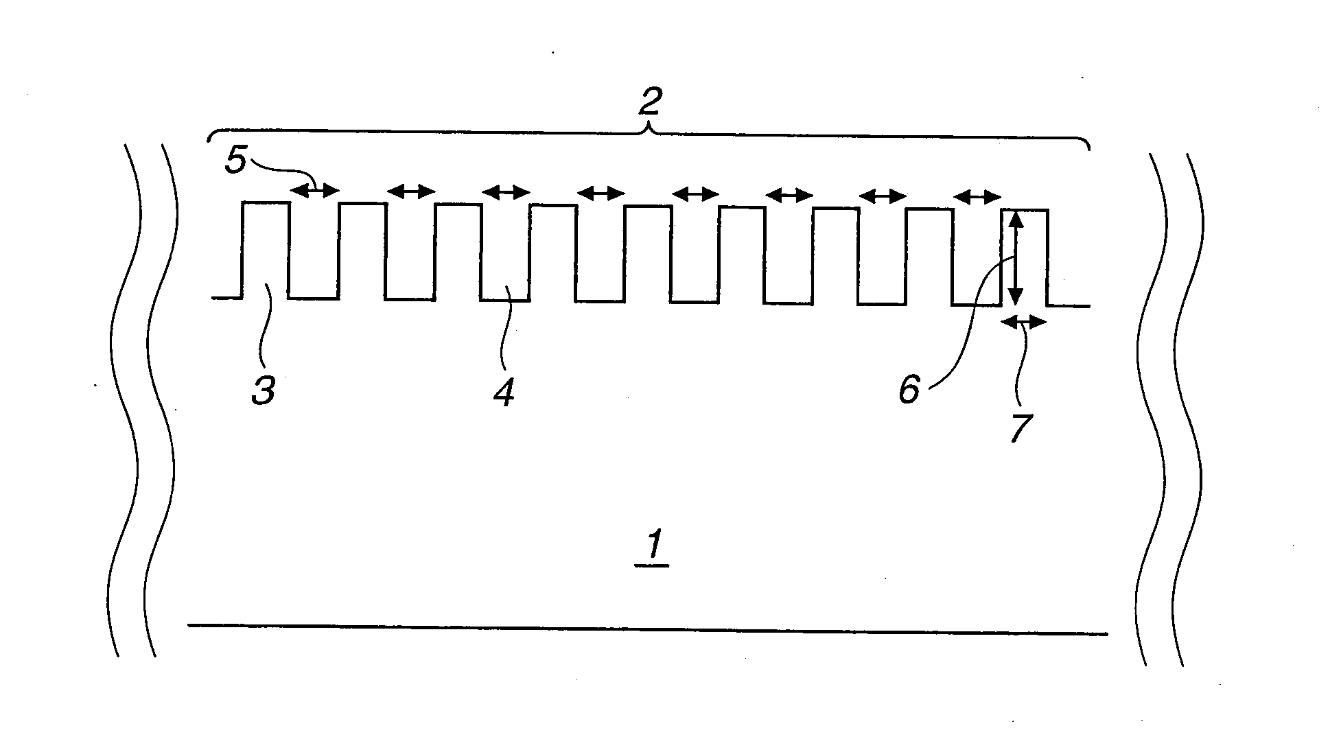
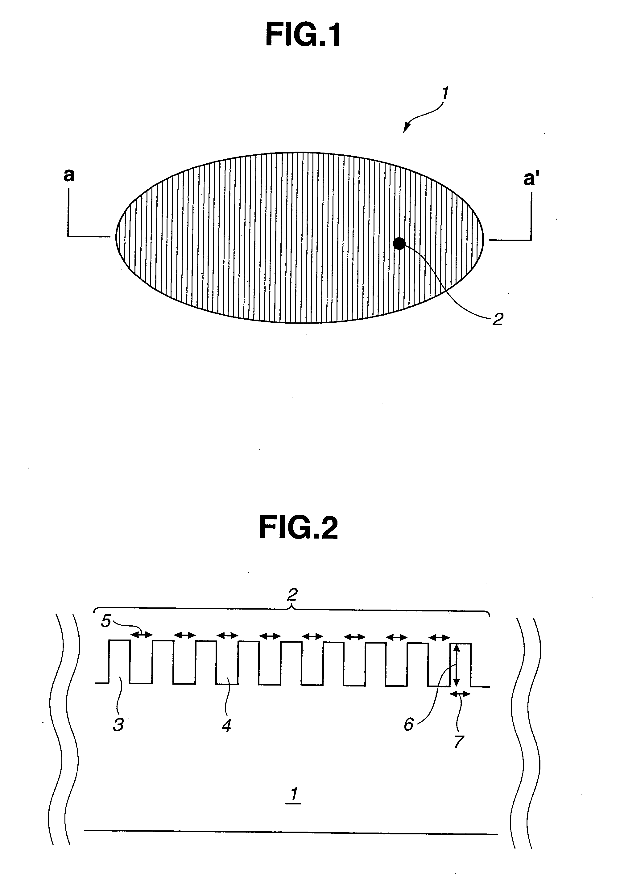
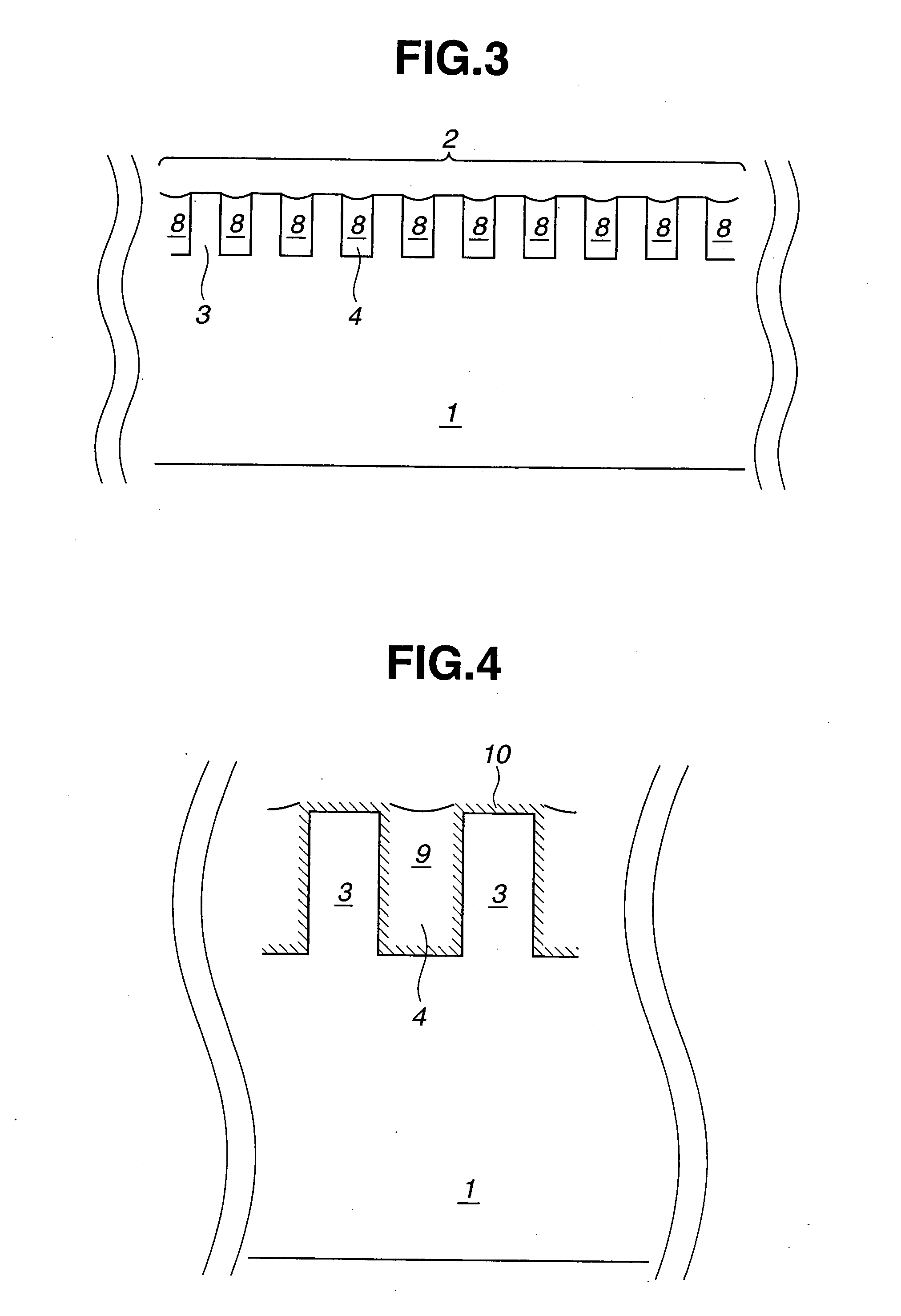
[0023]In the present invention, the water-repellent compound has a reactive moiety chemically bondable to Si element in the silicon wafer, and a hydrophobic group. With this, the surface of the silicon wafer can keep the surface condition provided with water repellency until the cleaning agent is removed from the recessed portion. Since the surface of the recessed portion is under the condition provided with water repellency when the cleaning liquid is removed or dried, the capillary force is so reduced that the pattern collapse becomes hard to occur. If the capillary force of the surface of the recessed portion on the assumption that water is retained in the recessed portion of the surface of the silicon wafer provided with water repellency is not larger than 2.1 MN / m2, the capillary force is so small as not to cause the pattern collapse and therefore preferable. Additionally, the surface condition provided with water repellency can be removed by at least one treatment selected from irradiation with light, heating of the silicon wafer, and exposing the silicon wafer to ozone.
[0024]Additionally, in the water-repellent cleaning liquid in the first cleaning agent, the water-repellent compound having a reactive moiety chemically bondable to Si element in the silicon wafer and a hydrophobic group and the alcoholic solvent are mixed and contained. With this, the surface of the recessed portion can readily reach the surface condition sufficiently provided with water repellency, in a short time.
[0025]In the water-repellent cleaning liquid, a water-repellent compound of less than 0.1 mass % relative to the total quantity of 100 mass % of the water-repellent cleaning liquid makes the surface of the recessed portion hard to reach the surface condition sufficiently provided with water repellency. Meanwhile, a water-repellent compound exceeding 99.9 mass % lessens the effect of alcohol (with which water repellency can be sufficiently imparted to the surface of the recessed portion in a short time).

Problems solved by technology

On the other hand, in cleaning conventionally performed with a mixed ammonia cleaning agent, damages to the wafer due to its basicity are getting serious with the trend toward micro-patterning for circuits.
With this, problems about the damages to the wafer due to cleaning have been solved; however, problems due to an aspect ratio increased with the trend toward micro-processing in the semiconductor devices have become obvious.
In other words, a phenomenon where the pattern collapses when a gas-liquid interface passes through the pattern is brought about after cleaning or rinsing to largely reduce the yield, which has become a significant problem.
This method is effective for preventing the pattern collapse; however, a solvent having small γ such as 2-propanol and the like is also small in normal contact angle, which results in the trend to increase cos θ. It is therefore said that there are limitations to adaptable patterns, for example, an aspect ratio of not higher than 5.
However, the thus disclosed technique cannot be applied to the present object, because: it is directed to the resist pattern or for reforming a resist itself; and a final removal together with the resist is possible so as not to need the assumption about a method of removing a treatment agent after drying.
However, any of these needs a treatment in a closed system or a batch in contrast to the conventional cleaning processes and therefore involves issues in view of cost such as throughput, though effective to some extent.

Method used


Image

  • Cleaning Agent For Silicon Wafer
  • Cleaning Agent For Silicon Wafer
  • Cleaning Agent For Silicon Wafer

Examples


example 16

[0150]The manner was all the same as Example 14 with the exception that CTFP was used as the organic solvent other than the alcoholic solvent in the water-repellent cleaning liquid. As shown in the evaluation result of Table 1, the contact angle after the surface treatment was 72° and therefore the water repellency-providing effect was exhibited. Additionally, the capillary force at the time where water was retained was 1.0 MN / m2 and therefore the capillary force was small. Additionally, the contact angle after UV irradiation was smaller than 10°, so that removal of the water repellency-provided surface condition was achieved. Furthermore, the Ra value of the wafer after UV irradiation was smaller than 0.5 nm, with which it was confirmed that the wafer was not eroded at the time of cleaning and that the residue of the water-repellent cleaning liquid did not remain after UV irradiation.

example 17

[0151]The manner was all the same as Example 15 with the exception that 1-propanol (nPA) was used as the alcoholic solvent. As shown in the evaluation result of Table 1, the contact angle after the surface treatment was 80° and therefore the water repellency-providing effect was exhibited. Additionally, the capillary force at the time where water was retained was 0.6 MN / m2 and therefore the capillary force was small. Additionally, the contact angle after UV irradiation was smaller than 10°, so that removal of the water repellency-provided surface condition was achieved. Furthermore, the Ra value of the wafer after UV irradiation was smaller than 0.5 nm, with which it was confirmed that the wafer was not eroded at the time of cleaning and that the residue of the water-repellent cleaning liquid did not remain after UV irradiation.

example 18

[0152]The manner was all the same as Example 17 with the exception that CTFP was used as the organic solvent other than the alcoholic solvent in the water-repellent cleaning liquid. As shown in the evaluation result of Table 1, the contact angle after the surface treatment was 78° and therefore the water repellency-providing effect was exhibited. Additionally, the capillary force at the time where water was retained was 0.7 MN / m2 and therefore the capillary force was small. Additionally, the contact angle after UV irradiation was smaller than 10°, so that removal of the water repellency-provided surface condition was achieved. Furthermore, the Ra value of the wafer after UV irradiation was smaller than 0.5 nm, with which it was confirmed that the wafer was not eroded at the time of cleaning and that the residue of the water-repellent cleaning liquid did not remain after UV irradiation.


PUM

PropertyMeasurementUnit
Percent by massaaaaaaaaaa
Pressureaaaaaaaaaa

Abstract

A cleaning agent for a silicon wafer (a first cleaning agent) contains at least a water-based cleaning liquid and a water-repellent cleaning liquid for providing at least a recessed portion of an uneven pattern with water repellency during a cleaning process. The water-based cleaning liquid is a liquid in which a water-repellent compound having a reactive moiety chemically bondable to Si element in the silicon wafer and a hydrophobic group, and an organic solvent including at least an alcoholic solvent are mixed and contained. With this cleaning agent, the cleaning process which tends to induce a pattern collapse can be improved.

Description

TECHNICAL FIELD[0001]The present invention relates to a technique of cleaning a silicon substrate (a wafer) in production of semiconductor devices, the purpose of which being production yield improvements of devices having such a circuit pattern as to be particularly fine and particularly high in aspect ratio.BACKGROUND OF THE INVENTION[0002]Semiconductor devices for use in networks or digital household electric appliances are being further desired to be sophisticated, multifunctional, and low in power consumption. Accordingly, the trend toward micro-patterning for circuits has been developed, with which micro-sizing of particles has advanced to cause reduction in production yield. As a result of this, a cleaning process for the purpose of removing the micro-sized particles is frequently used. As a result of this, 30-40% of the whole of the semiconductor fabrication process is occupied with the cleaning process.[0003]On the other hand, in cleaning conventionally performed with a mix...

Claims


Application Information

Patent Timeline
IPC IPC(8): B08B3/00C11D3/20
CPCB08B3/00C11D7/5022H01L21/00C09D183/04H01L21/02052H01L21/02054C11D3/162
Inventor KUMON, SOICHISAIO, TAKASHIARATA, SHINOBUNANAI, HIDEHISAAKAMATSU, YOSHINORIHAMAGUCHI, SHIGEOMAEDA, KAZUHIKO
Owner CENT GLASS CO LTD
Learn More