Semiconductor device

a technology of semiconductors and devices, applied in the direction of semiconductor devices, basic electric elements, electrical equipment, etc., can solve the problems of limitations in reducing the leakage current flowing on the surface using the conventional art, and achieve the effect of reducing the leakage curren

Inactive Publication Date: 2011-10-27
SUMITOMO ELECTRIC IND LTD
View PDF7 Cites 7 Cited by
  • Summary
  • Abstract
  • Description
  • Claims
  • Application Information

AI Technical Summary

Benefits of technology

[0007]The present invention has been made in view of the foregoing problem, and its object is to provide a semiconductor device having reduced leakage current flowing in an interface between a protective film and a silicon carbide layer.
[0009]According to the present invention, the surface at which the depletion layer faces the protective film includes the portion having an off angle of 10° relative to the {0-33-8} plane, i.e., portion with a particularly small interface state density. This restrains generation of leakage current resulting from the interface state, thereby obtaining a semiconductor device with a small leakage current.
[0011]Preferably, an interface between the portion of the surface of the silicon carbide layer and the protective film has an interface state density of not more than 5×1012 cm2 eV−1. Accordingly, the surface at which the depletion layer faces the protective film includes a portion with a particularly small interface state density. This restrains generation of leakage current resulting from the interface state, thereby obtaining a semiconductor device with a small leakage current.
[0012]Preferably, the interface between the portion of the surface of the silicon carbide layer and the protective film contains nitrogen atoms. Accordingly, the interface state density is further reduced. This restrains generation of the leakage current resulting from the interface state, thereby obtaining a semiconductor device with a small leakage current.
[0014]Preferably, the substrate includes a first layer facing the silicon carbide layer and a second layer supporting the first layer, and the second layer has an impurity concentration larger than that of the first layer. Accordingly, the conductivity of the second layer becomes large, thereby reducing on-resistance of the semiconductor device.
[0015]Preferably, the first layer has a threading dislocation density smaller than that of the second layer. This can reduce the threading dislocation density of the surface on which the silicon carbide layer is formed, thereby forming a silicon carbide layer with higher quality.

Problems solved by technology

However, even if such a protective film is formed, there are limitations in reducing the leakage current flowing on the surface using the conventional art.

Method used


Image

  • Semiconductor device
  • Semiconductor device
  • Semiconductor device

Examples


first embodiment

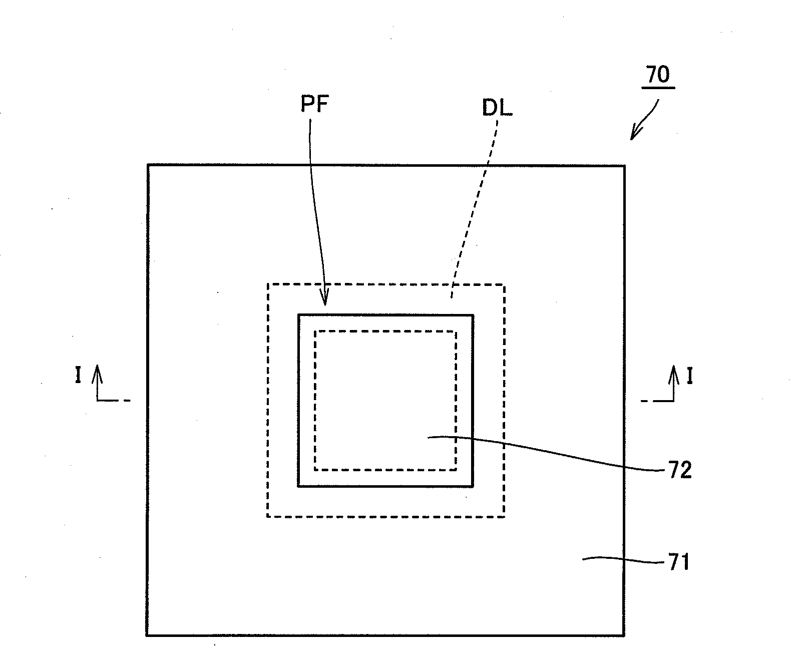
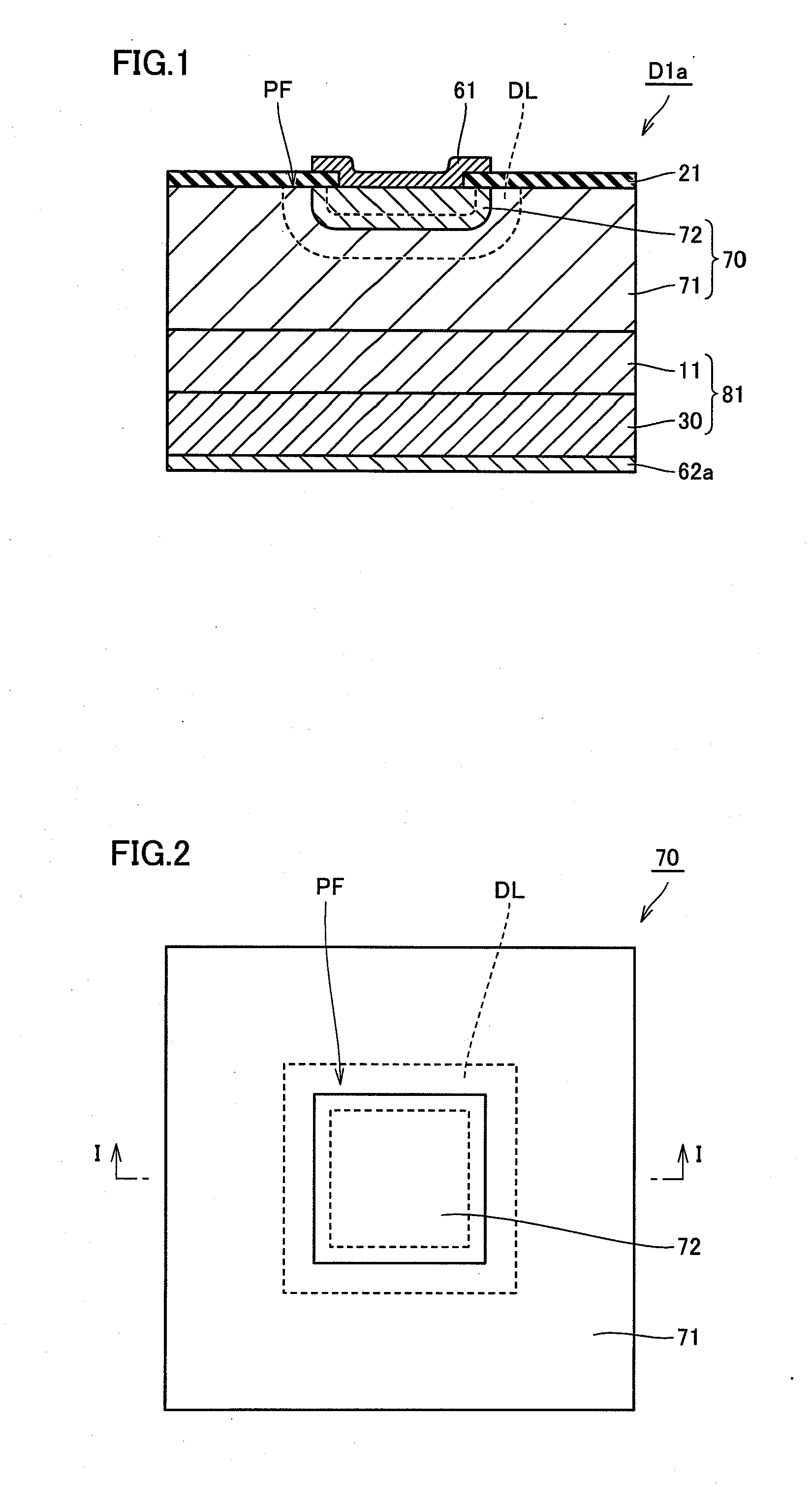
[0032]Referring to FIG. 1 and FIG. 2, a diode D1a (semiconductor device) of the present embodiment is a diode having a rectifying function provided by a depletion layer DL and having a planar structure. Diode D1a has a cathode electrode 62a, a substrate 81, a silicon carbide layer 70, a protective film 21, and an anode electrode 61.

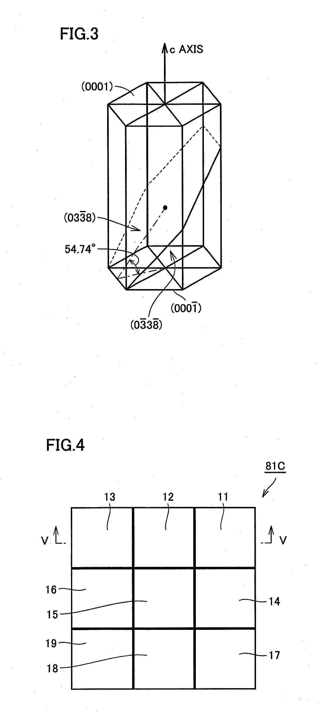
[0033]Substrate 81 is made of silicon carbide. Substrate 81 has a high-quality layer (first layer) 11 and a base layer (second layer) 30. High-quality layer 11 faces silicon carbide layer 70. Further, high-quality layer 11 has a hexagonal single-crystal structure (FIG. 3), and has a plane orientation of {0-33-8}. This single-crystal structure has a polytype of, for example, 4H. Base layer 30 supports high-quality layer 11. High-quality layer 11 has a threading dislocation density smaller than that of base layer 30. An Impurity is added to base layer 30 and high-quality layer 11 to provide them with the same conductive type. Base layer 30 has an impurity c...

second embodiment

[0055]Referring to FIG. 8, a diode D1b (semiconductor device) of the present embodiment is a lateral type diode unlike diode D1a (FIG. 1), and has a cathode electrode 62b instead of cathode electrode 62a. Cathode electrode 62b is provided on n− layer 71. According to the present embodiment, an effect similar to that in the first embodiment can be obtained in diode D1b of lateral type.

[0056]In order to reduce contact resistance of cathode electrode 62b, a contact portion of n− layer 71 with cathode electrode 62b may be provided with a region having a high impurity concentration (not shown). Such a region can be formed by, for example, ion implantation.

third embodiment

[0057]Referring to FIG. 9-FIG. 11, a diode D2a (semiconductor device) of the present embodiment is a diode having a rectifying function provided by depletion layer DL, and having a mesa structure. Diode D2a has a cathode electrode 62a, a substrate 82, a silicon carbide layer 70N, a protective film 21N, and an anode electrode 61.

[0058]Substrate 82 is made of silicon carbide having a hexagonal single-crystal structure (FIG. 3). This single-crystal structure has a polytype of, for example, 4H. Further, substrate 82 has one surface facing silicon carbide layer 70N and having a plane orientation of {0001}. The other surface of substrate 82 faces cathode electrode 62a.

[0059]Silicon carbide layer 70N is epitaxially grown on substrate 82 and is accordingly formed thereon, and has a hexagonal single-crystal structure (FIG. 3). Further, silicon carbide layer 70N has an if layer 71N and a p layer 72N. N− layer 71N faces substrate 82, and has the same conductive type as that of substrate 82. P...


PUM

PropertyMeasurementUnit
off angleaaaaaaaaaa
off angleaaaaaaaaaa
off angleaaaaaaaaaa

Abstract

A silicon carbide layer is provided on a substrate, has a hexagonal single-crystal structure, and has a surface at which a depletion layer is formed. A protective film is insulative and provided on the silicon carbide layer to directly cover the surface. The surface thus directly covered with the protective film includes a portion having an off angle of not more than 10° relative to the {0-33-8} plane of the silicon carbide layer. This results in reduced leakage current flowing in an interface between the protective film and the semiconductor layer.

Description

BACKGROUND OF THE INVENTION[0001]1. Field of the Invention[0002]The present invention relates to a semiconductor device having a silicon carbide layer.[0003]2. Description of the Background Art[0004]In recent years, substrates made of silicon carbide (SiC) having a hexagonal crystal structure have been adopted as semiconductor substrates for use in manufacturing semiconductor devices. Such a substrate is usually manufactured by slicing a SiC ingot obtained by growth in the {0001} plane, which is less likely to cause stacking fault. Hence, SiC substrates having plane orientations close to the {0001} plane are widely used.[0005]For example, Japanese Patent Laying-Open No. 2009-088223 discloses a pn junction diode having a planar structure and utilizing a SiC substrate having a plane orientation inclined by eight degrees relative to the {0001} plane.[0006]In a semiconductor device which utilizes a depletion layer formed in a silicon carbide layer to interrupt a current, one of methods ...

Claims


Application Information

Patent Timeline
Patent Type & Authority Applications(United States)
IPC IPC(8): H01L29/24
CPCH01L29/045H01L29/1608H01L29/8613H01L29/8611H01L29/6606
Inventor HIYOSHI, TORUWADA, KEIJIMASUDA, TAKEYOSHI
Owner SUMITOMO ELECTRIC IND LTD
Why Eureka
Try Eureka