
All-digital clock data recovery device and transceiver implemented thereof

Inactive Publication Date: 2011-11-03
SEOUL NAT UNIV R&DB FOUND +1
View PDF1 Cites 24 Cited by
  • Summary
  • Abstract
  • Description
  • Claims
  • Application Information

AI Technical Summary

Benefits of technology

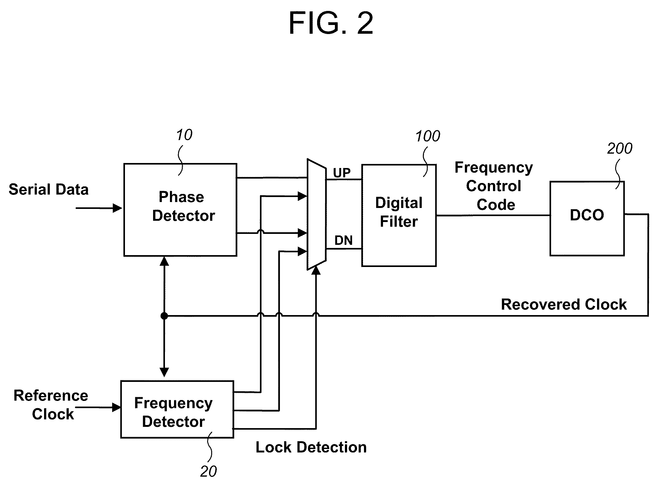
[0015]Another goal of the present invention is to provide a method and configuration architecture implemented thereof for eliminating the jitters due to the quantization errors and for resolving the inherent problem of the sluggish operation of digital filters when the conventional CDR circuitry including the charge pump circuit as well as the voltage controlled oscillator is to be converted into the digital circuitry either via digital filters or via digital circuits.
[0016]Additional goal of the present invention is to provide a method and circuit implemented thereof for minimizing the hardware size of the circuit block of the digitally controlled oscillator (DCO), for reducing the generation of glitches, and for equalizing tuning steps in the frequency scale.

Problems solved by technology

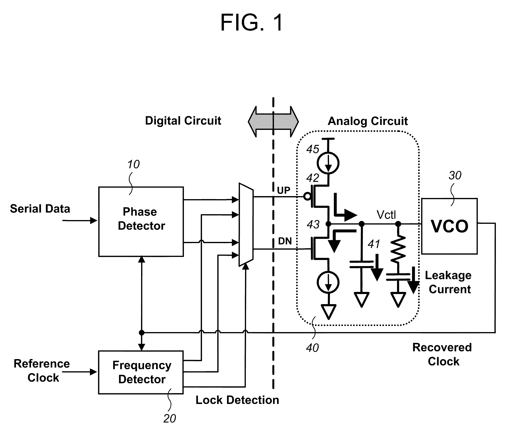
If the thickness of the gate oxide film is reduced down to the scale of nanometer, the current leakage problem becomes significant in the capacitors (41) comprising the charge pump circuits (40).
Consequently, it is not easy to restore a clock by fine-tuning in the nanometer-scaled integrated circuit since the voltage controlling the voltage controlled oscillator (30) is varied by the leakage current.
Furthermore, since the power supply for the 100 nanometer design rule is less than 1.0 V, it is impossible to implement the current sources (45) for the charge pump circuit (40) in the 100 nanometer-scaled semiconductor integrated circuit.
Therefore, we find some difficulties in implementing the analog charge pump circuits in the sub-100 nanometer integrated circuits, which has a constraint in the power supply voltage wherein the power supply voltage should be less than 1.0 V.

Method used


Image

  • All-digital clock data recovery device and transceiver implemented thereof
  • All-digital clock data recovery device and transceiver implemented thereof
  • All-digital clock data recovery device and transceiver implemented thereof

Examples


Embodiment Construction

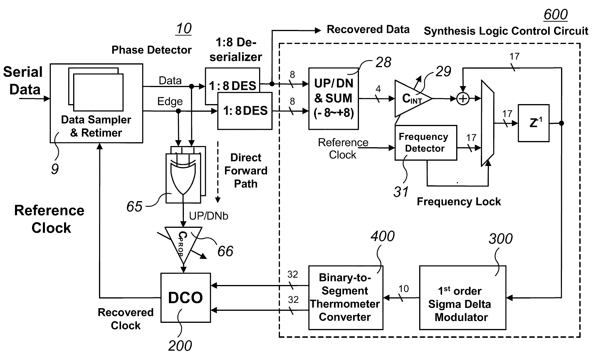
[0030]As a preferred embodiment of the present invention, a variable resistance switching matrix is implemented by PMOS transistor arrays wherein the PMOS transistors act as variable resistors since the amount of conducting current is controlled by the input gate voltage. The present invention proposes an approach of inserting vertical resistances between the rows of the switching matrix in order to equalize the frequency tuning steps both at high levels and at low levels. Obviously, the vertical resistance is implemented by a PMOS transistor while the gate is grounded.

[0031]In addition, the present invention employs 1st ΣΔ (sigma-delta) modulator to implement the dithering algorithm in an effort to resolve the jitter noise problem which is caused by the quantization errors when comparison is made between digitally controlled oscillator (DCO) and voltage controlled oscillator (VCO) of analog type. For instance, the present invention prevents the generation of quantization errors for...


PUM


Abstract

The present invention relates to an all-digital clock data recovery (CDR) which is implemented by a digital filter and a digitally controlled oscillator. The CDR of the present invention comprises a phase detector producing a digital sequence of data and a digital sequence of edge by sampling the serial data stream with a clock, a de-serializer transforming the digital sequences of data and edge into n-bit bus, a digitally controlled oscillator (DCO) implemented by a multi-stage chain of inverters having a variable resistance switching matrix wherein the resistance of each element of the variable resistance switching matrix is varied in such a way that the supply current being fed to each inverter is controlled in pursuant to a digital control code, and thereby producing a clock whose oscillation frequency is updated and fed to the phase detector, a digital synthesis control logic circuit generating a thermometer-code-type digital control code out of the n-bit data and n-bit edge from the de-serializer wherein the thermometer-code-type digital control code is fed to the DCO, and a 2-bit direct forward path directly controlling the frequency of the clock being produced by the DCO with an operating speed which is faster than the digital synthesis control logic circuit by n times.

Description

CROSS REFERENCE TO RELATED APPLICATION[0001]This application claims priority under 35 USC §119 to PCT Application No. PCT / KR2009 / 000321, filed on Jan. 22, 2009, the contents of which are incorporated herein by reference in their entirety.FIELD OF THE INVENTION[0002]The present invention relates to a Clock Data Recovery (CDR) restoring a clock and data from the received data bit stream in the serial data communication, and a transceiver implemented thereof, and more particularly the all-digital circuit technology for implementing the CDR device without any analog part.BACKGROUND OF THE INVENTION[0003]Recently, a serial link transceiver tends to be integrated in a single chip due to the boosting utilization of the high-speed serial link which can transmit gigabits per second. The sender transmits only the data stream without a clock to the receiver through the communication channel in the chip-to-chip communication. A clock and data recovery, which extracts a clock and data from the t...

Claims


Application Information

Patent Timeline
IPC IPC(8): H03K5/00
CPCH03L7/0807H03L7/0995H04L7/0331H04L7/033H04L7/0079H03L7/093H03L7/099H04B1/06
Inventor JEONG, DEOG KYOONOH, DO HWAN
Owner SEOUL NAT UNIV R&DB FOUND
Learn More