Group 3B nitride crystal substrate

a nitride crystal and substrate technology, applied in the direction of crystal growth process, crystal growth process, polycrystalline material growth, etc., can solve the problem of inability to obtain high-quality gallium nitride crystals, etc., and achieve high color rendering properties and high quality

Active Publication Date: 2011-11-10
NGK INSULATORS LTD
View PDF3 Cites 17 Cited by
  • Summary
  • Abstract
  • Description
  • Claims
  • Application Information

AI Technical Summary

Benefits of technology

[0006]An object of the present invention is to provide a group 13 nitride crystal substrate of high quality produced by growing a group 13 nitride crystal on a seed-crystal substrate by a flux method.
[0009]A group 13 nitride crystal substrate according to the present invention has a considerably lower content of inclusions than existing group 13 nitride crystal substrates and hence can be applied to technical fields that demand high quality, for example, to white LEDs that have high color-rendering properties and are expected to replace fluorescent lamps, violet laser discs for high-speed high-density optical storages, and power devices used for inverters for hybrid vehicles.

Problems solved by technology

However, when the growth rate of a gallium nitride crystal is made high as in Patent Literature 1, there are cases where the content of inclusions (solidified matter that is derived from the melt mixture incorporated into gallium nitride) increases and a gallium nitride crystal of high quality cannot be obtained.

Method used


Image

  • Group 3B nitride crystal substrate
  • Group 3B nitride crystal substrate
  • Group 3B nitride crystal substrate

Examples


example 1

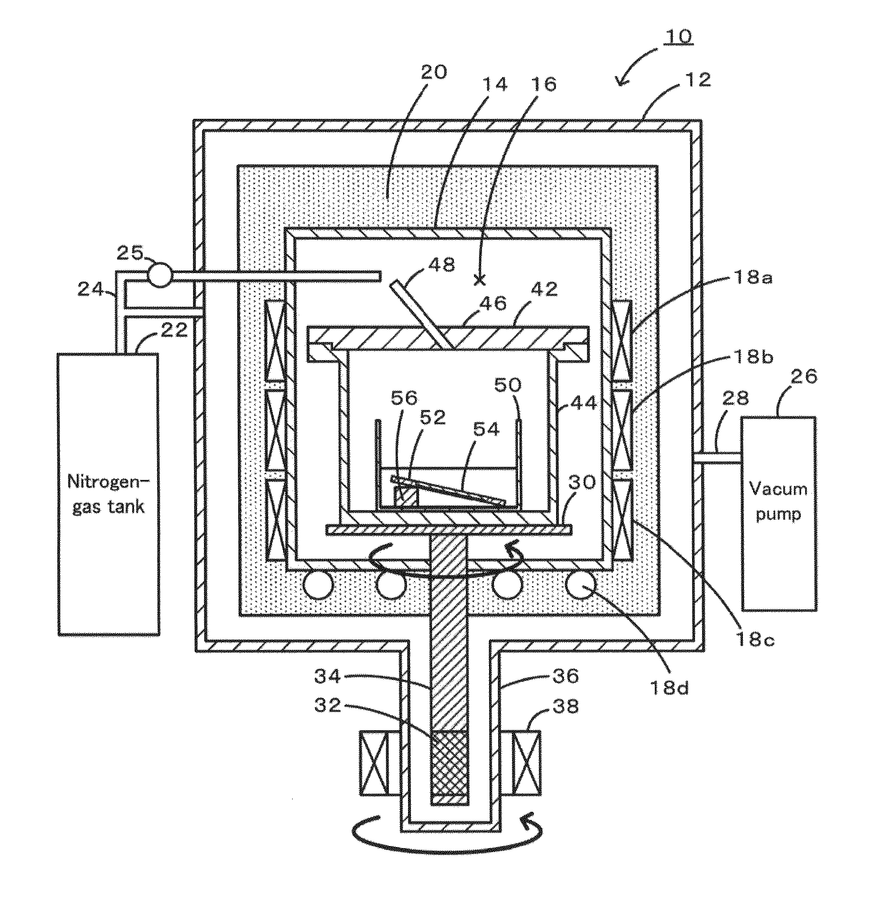
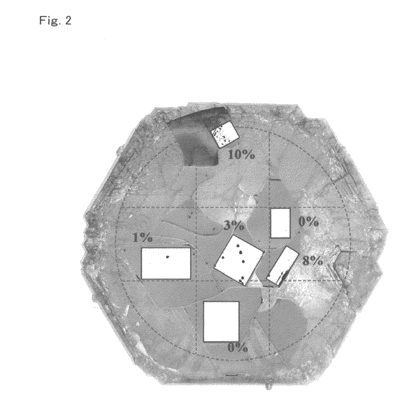
[0033]A gallium nitride crystal substrate was produced with the crystal substrate production apparatus 10 illustrated in FIG. 1. Hereinafter, the production procedures will be described. The tray support 56 was placed in a marginal portion within the growth vessel 50 having an internal diameter of 100 mm within a glove box having an argon atmosphere. The seed-crystal-substrate tray 52 was placed so as to lean on the tray support 56, at an angle of 10° in the center of the bottom surface of the growth vessel 50. A GaN template having a diameter of 3 inches was placed as the seed-crystal substrate 54 in the center of the seed-crystal-substrate tray 52. Furthermore, 110 g of sodium metal, 130 g of gallium metal, and 300 mg of carbon were added into the growth vessel 50. The growth vessel 50 was put into the outer-container body 44. The opening of the outer-container body 44 was closed with the outer-container lid 46 equipped with the nitrogen introduction pipe 48. The outer container 4...

example 2

[0036]A gallium nitride crystal was grown under the same conditions as those in EXAMPLE 1 except that the outer container 42 was rotated at 1 rpm. The obtained gallium nitride crystal substrate had a diameter of 3 inches and a thickness of about 750 μm. The crystal growth rate was about 5 μm / h. The gallium nitride crystal substrate was also measured in terms of the inclusion content of the five segments as in EXAMPLE 1 and the inclusion content was found to be 0 to 10%. Irradiation with light from a mercury lamp resulted in emission of blue fluorescence. The dislocation density was 1×10⁴ / cm2.

example 3

[0037]A gallium nitride crystal was grown under the same conditions as those in EXAMPLE 1 except that the outer container 42 was rotated at 5 rpm. The obtained gallium nitride crystal substrate had a diameter of 3 inches and a thickness of about 1 mm. The crystal growth rate was about 7 μm / h. The gallium nitride crystal substrate was also measured in terms of the inclusion content of the five segments as in EXAMPLE 1 and the inclusion content was found to be 0 to 1%. Irradiation with light from a mercury lamp resulted in emission of blue fluorescence. The dislocation density was 2×10⁴ / cm2.


PUM

PropertyMeasurementUnit
temperaturesaaaaaaaaaa
pressureaaaaaaaaaa

Abstract

A group 13 nitride crystal substrate according to the present invention is produced by growing a group 13 nitride crystal on a seed-crystal substrate by a flux method, wherein a content of inclusions in the group 13 nitride crystal grown in a region of the seed-crystal substrate except for a circumferential portion of the seed-crystal substrate, the region having an area fraction of 70% relative to an entire area of the seed-crystal substrate, is 10% or less, preferably 2% or less.

Description

FIELD OF THE INVENTION[0001]The present invention relates to a crystal substrate of a group 13 nitride such as gallium nitride.BACKGROUND OF THE INVENTION[0002]In recent years, production of semiconductor devices such as blue LEDs, white LEDs, and violet semiconductor lasers by using group 13 nitrides such as gallium nitride and application of such semiconductor devices to various electronic apparatuses have been actively studied. Existing gallium nitride semiconductor devices are mainly produced by vapor-phase methods: specifically, by heteroepitaxial growth of a gallium nitride thin film on a sapphire substrate or a silicon carbide substrate by a metal-organic vapor phase epitaxy method (MOVPE) or the like. In this case, since such a substrate and the gallium nitride thin film are considerably different from each other in terms of thermal expansion coefficient and lattice constant, dislocations (one type of lattice defects in crystals) are generated at a high density in the galliu...

Claims


Application Information

Patent Timeline
Patent Type & Authority Applications(United States)
IPC IPC(8): C01B21/06C30B19/04C30B19/02
CPCC30B9/12C30B29/406C30B29/403
Inventor SHIMODAIRA, TAKANAOIMAI, KATSUHIROIWAI, MAKOTOHIRAO, TAKAYUKI
Owner NGK INSULATORS LTD
Why Eureka
Try Eureka