Otft using paper as substrate and silk protein as insulating material and method for manufacturing the same

a technology silk protein, which is applied in the field of organic thin film transistor (otft), can solve the problems of pentacene not matching well with the conventional dielectric material, the sputtering process instrument is very expensive, and the process is complex, and achieves high performan

Inactive Publication Date: 2011-12-01
NATIONAL TSING HUA UNIVERSITY
View PDF5 Cites 11 Cited by
  • Summary
  • Abstract
  • Description
  • Claims
  • Application Information

AI Technical Summary

Benefits of technology

[0010]The object of the present invention is to provide an OTFT and a method for manufacturing the same to prepare an OTFT with flexibility, rollability and high performance.
[0013]According to the OTFT and the method for manufacturing the same of the present invention, the paper substrate with a gate electrode formed thereon is coated with a silk solution to form a gate insulating layer containing silk protein. Compared to the conventional method for forming the gate insulating layer through a sputtering process or a vacuum deposition process, the method of the present invention can be performed in a solution process. Hence, the process of the present invention is low cost and simple, and can be used for preparing the OTFT with large area. Also, the silk protein is low cost and easily available. In addition, the silk protein used in the OTFT of the present invention matches well with the material of the organic semiconductor layer, so the transistor characteristics of the OTFT can be greatly improved. Furthermore, paper, which is inexpensive and can be easily accessible, is used as a substrate, so the resulting OTFT has the advantages of flexibility, rollability, and foldability. Hence, the OTFT of the present invention can be applied to various fields, such as RFID. Also, the paper is an organic material which can be easily recycled. Compared to the OTFT with a plastic substrate, the environmental pollution can be solved by use of the OTFT of the present invention.

Problems solved by technology

However, the instrument for the sputtering process is very expensive and the process is complex.
However, pentacene cannot match well with the conventional dielectric material, so the carrier mobility of pentacene is low.
Hence, it is impossible to manufacture OTFTs with high performance by using the present techniques and materials.
Recently, the environmental protection has become a global issue and attracts attention of the public worldwide.
Although the plastic substrate can be used to form an OTFT with flexibility and rollabiltiy, it has the disadvantages of difficulty in recycling and causing environmental pollution.
However, when the paper substrate is used, the carrier mobility of the OTFT is low due to the restriction on the temperature of the process and the selection of the dielectric material.

Method used


Image

  • Otft using paper as substrate and silk protein as insulating material and method for manufacturing the same
  • Otft using paper as substrate and silk protein as insulating material and method for manufacturing the same
  • Otft using paper as substrate and silk protein as insulating material and method for manufacturing the same

Examples


embodiment 1

Top Contact OTFT

[Preparation of a Silk Solution]

[0026]First, 10 wt % of an aqueous solution of Na2CO3 was provided and heated. When the solution was boiling, silkworm cocoon (natural silk) was added thereto, and the solution was kept boiling for 30 min to remove sericin. Then, the silk without sericin was washed by deionized water to remove the alkali salt adhered on the silk. After a drying process, refined silk, i.e. fibroin, was obtained.

[0027]Next, the refined silk was added into 85 wt % of phosphoric acid (H3PO4) solution (20 ml), and the resulted solution was stirred until the refined silk was dissolved. Then, the phosphoric acid solution containing the refined silk was put into a membrane (Spectra / Por 3 membrane, molecular weight cutoff=14000) and dialyzed with water. The dialysis process was performed for 3 days to remove the phosphate ions. After the dialysis process is completed, a filter paper is used to filter out impurities, and an aqueous solution of fibroin is obtaine...

embodiment 2

Bottom Contact OTFT

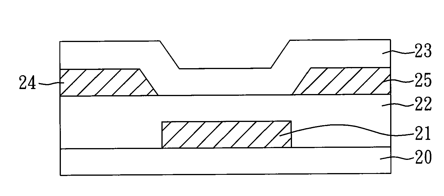
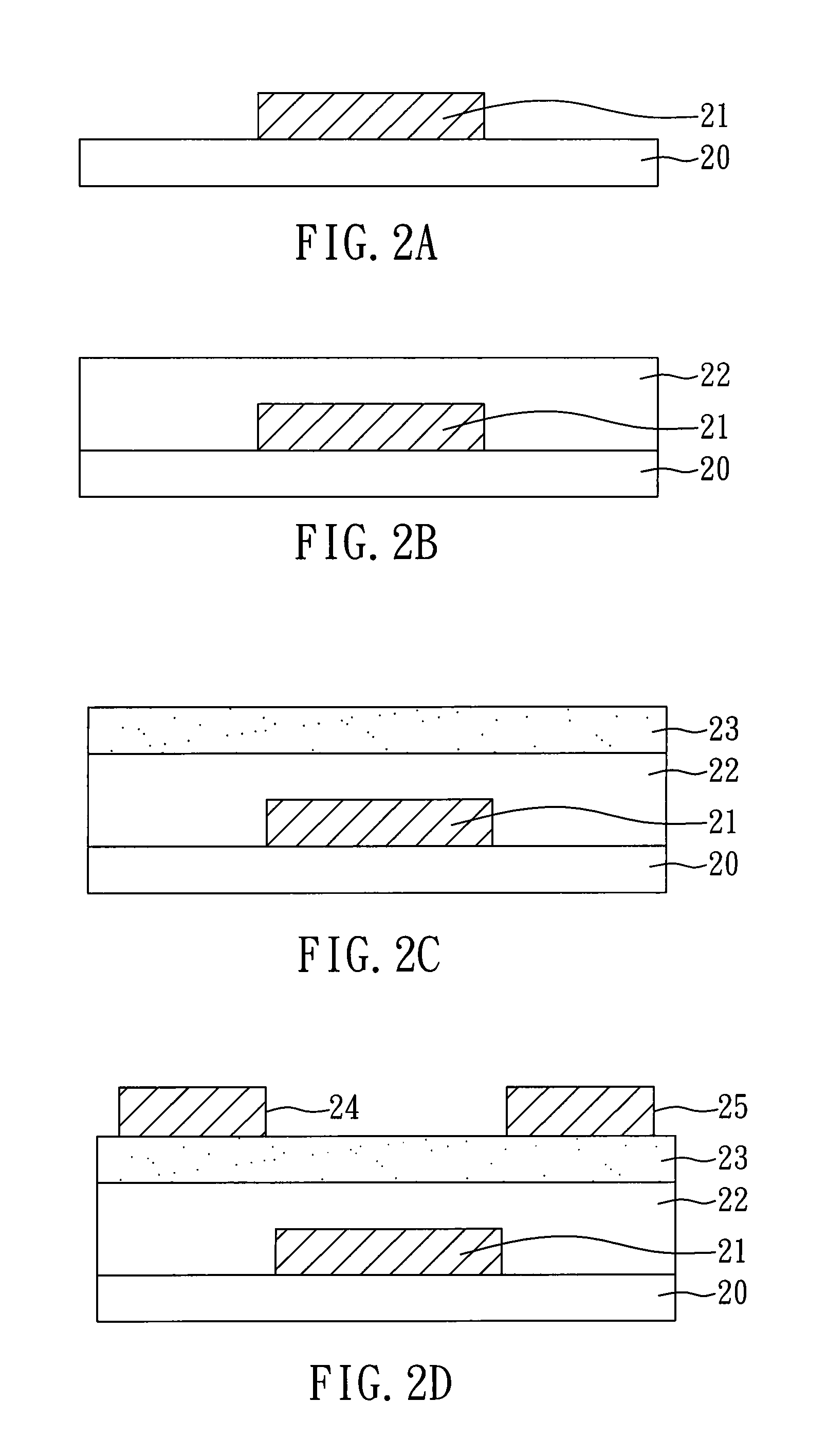
[0040]As shown in FIG. 5A, a paper substrate 20 was provided, and a gate electrode 21 and a gate insulating layer 22 was formed on the paper substrate 20 sequentially. In the present embodiment, the preparing methods and the materials of the paper substrate 20, the gate electrode 21, and the gate insulating layer 22 are the same as those illustrated in Embodiment 1. In addition, in the present embodiment, the thickness of the gate electrode 21 was about 100 nm, and the thickness of the gate insulating layer 22 was about 500 nm.

[0041]Next, the evaporation process was performed on the gate insulating layer 22 to form a patterned metal layer through the same evaporation process for forming the gate electrode described in Embodiment 1, wherein the patterned metal layer was used as a source electrode 24 and a drain electrode 25, as shown in FIG. 5B. In the present embodiment, the material of the source electrode 24 and the drain electrode 25 was Au, and the thickness o...


PUM


Abstract

An organic thin film transistor (OTFT) using paper as a substrate and silk protein as an insulating material and methods for manufacturing the same are disclosed. The OTFT of the present invention comprises: a paper substrate; a gate disposed on the paper substrate; a gate insulating layer containing silk protein, which is disposed on the paper substrate and covers the gate; an organic semiconductor layer; and a source and a drain, wherein the organic semiconductor layer, the source and the drain are disposed over the gate insulating layer.

Description

BACKGROUND OF THE INVENTION[0001]1. Field of the Invention[0002]The present invention relates to an organic thin film transistor (OTFT) and a method for manufacturing the same and, more particularly, to an OTFT and method for manufacturing the same which use paper as a substrate and silk protein as an insulating material. Therefore, the OTFT of the present invention has the characteristics of flexibility and rollablity due to use of the paper substrate.[0003]2. Description of Related Art[0004]Thin film transistors (TFTs) are fundamental components in contemporary electronics, such as sensors, radio frequency identification (RFID) tags, and electronic display devices. In recent years, in order to reduce the production cost and increase the product application, organic thin film transistors (OTFTs) have been rapidly developed which have the advantages of low-cost and flexibility, and can be produced in large-area.[0005]The OTFTs can be divided into top contact OTFTs and bottom contact...

Claims


Application Information

Patent Timeline
Patent Type & Authority Applications(United States)
IPC IPC(8): H01L51/10H01L51/40
CPCB82Y10/00H01L51/0003H01L51/0055Y02E10/549H01L51/0097H01L51/052H01L51/0545H01L51/0093Y02P70/50H10K71/12H10K85/623H10K85/761H10K77/111H10K10/471H10K10/466
Inventor HWANG, JENN-CHANGWANG, CHUNG HWAHSIEH, CHAO YING
Owner NATIONAL TSING HUA UNIVERSITY
Why Eureka
Try Eureka